A related question is a question created from another question. When the related question is created, it will be automatically linked to the original question.
If you have a related question, please click the "Ask a related question" button in the top right corner. The newly created question will be automatically linked to this question.
I would like to switch the LM5642 circuit on and off only via the supply voltage VIN by means of a switch. The power path to the transistors should not be interrupted. The signals ON/ SSx are thereby on "HIGH". Is this possible?
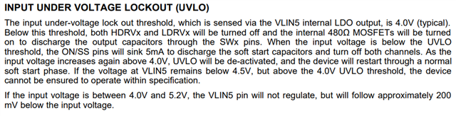
I believe the ON/SSX pins are internally pulled high, so just from toggling VIN on/off, you can place the device in and out of UVLO mode, which will restart the device automatically and undergo standard soft-start. What do you mean power path to the transistors should not be interrupted? Are the HS power FETs connected to a constant VDD source that is independent from VIN? If so, during UVLO, both HDRVx and LDRVx will be turned off, so FETs would not be switching.
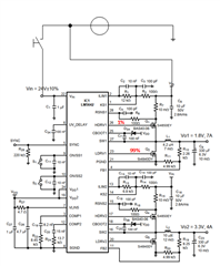
Hi henry, Thanks for your answer. To your questions: I want to switch the converter on/off via a small switch without interrupting the power path. Therefore I have divided the input voltage into two lines. One path goes via the current sense resistors to the high side transistors and the second path via a switch to VIN of the circuit. If I now interrupt the path to VIN, then with a PWM of about 99% the lower transistor is switched and with 1% the high side transistor. But the LM5642 is not really switched off, so that a small output voltage is still generated.
Thank you for your patience. It's recommended that the VIN be connected to both the IC and the FETs as indicated in the device datasheets. What is your reasoning for placing the disconnect onto the IC VIN line as opposed to toggling the EN/SS pins?