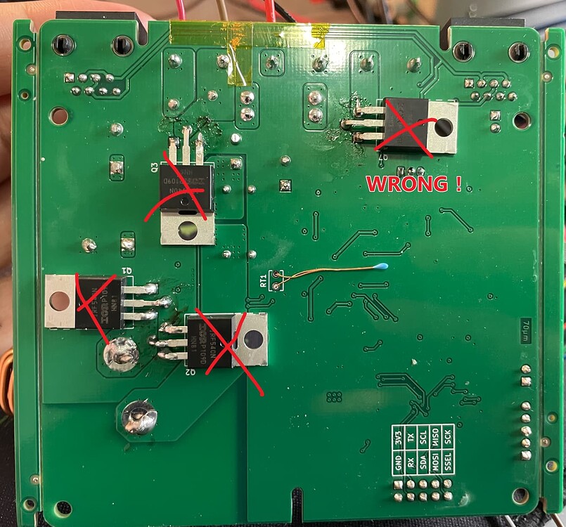
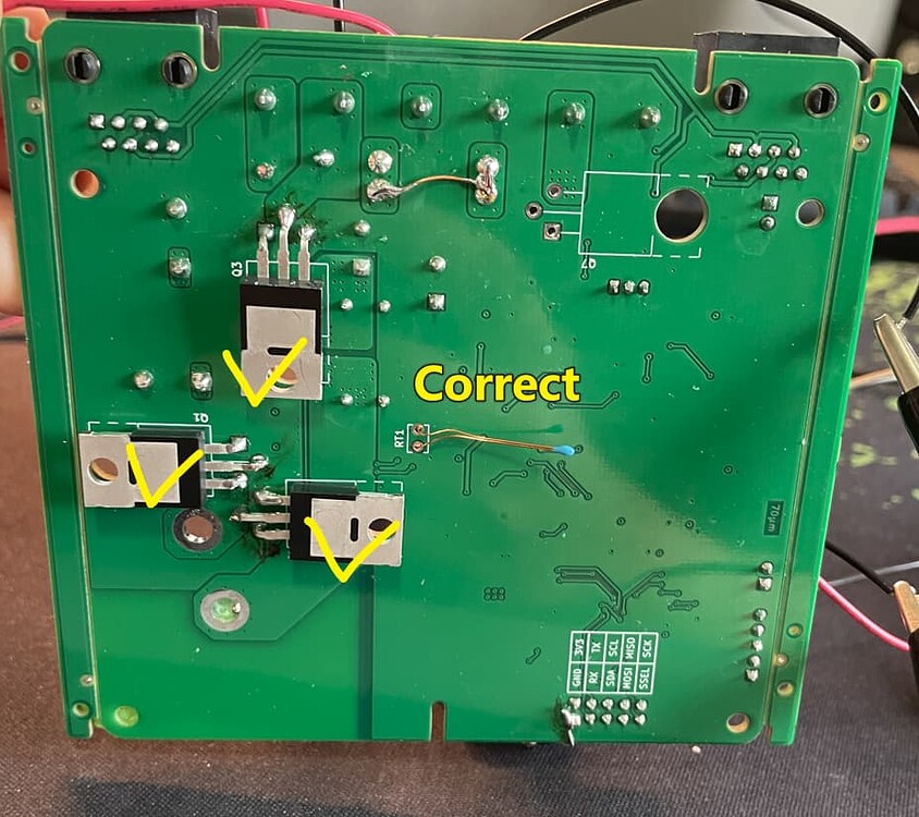
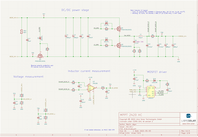
The schematic is like this:
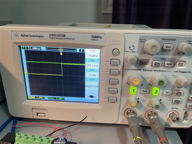
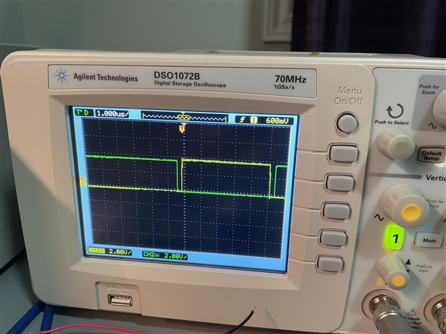
The following picture shows the input signal to the gate driver. Yellow is input of high side, Green is input of low side from mcu.
In the following picture yellow is the input of high side and green is the output of low side measured at R2. Signal feeding into the gate driver is same as shown in picture 1.
Probe at high side input and R1, the yellow signal below is high side input, the green signal is high side output. Low side input was feeding same signal as shown in Picture 1. High side output is always 12V while is should be HS voltage + 12v.