This thread has been locked.

If you have a related question, please click the "Ask a related question" button in the top right corner. The newly created question will be automatically linked to this question.

TPS54302:

Part Number: TPS54302

Hello,

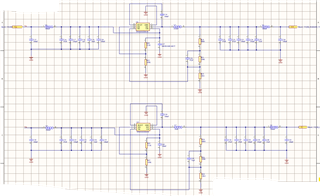
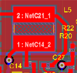
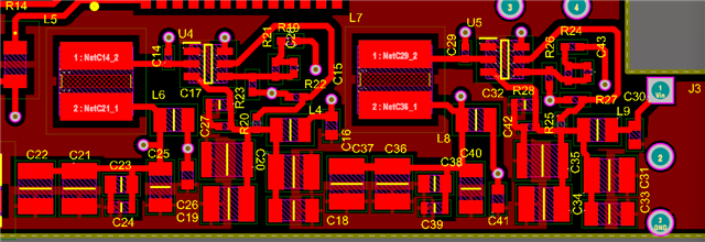
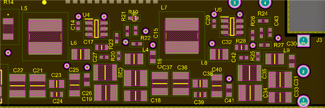
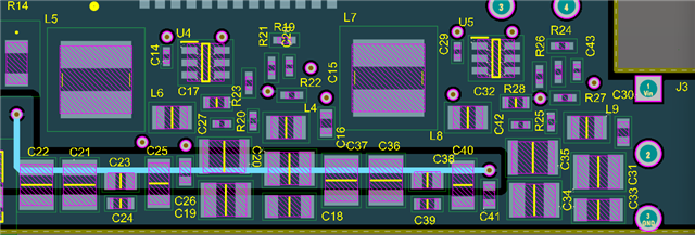
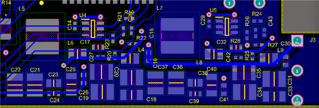
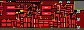
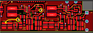
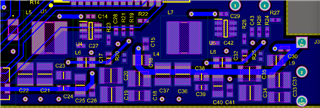
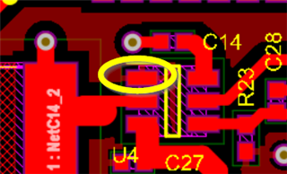
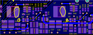
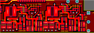
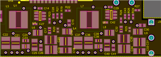
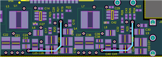
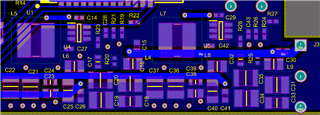
I have used two TPS54302 chips in my design to generate two voltage sources 5V DC and 3V3 DC from a common source Vin ( range from 7V DC to 24V DC, 3A).

I have done several tests and see that I can obtain 5V DC and 3V3 DC with some ripples ( around 40mV on 3V3 and around 120mV on 5V).

The problems that I have noticed are:

1- I cannot draw more than around 200mA from these voltage sources.

2- Drawing currents from each source (5V or 3V3) alone or both at the same time  would affect the level of output. 5V changes to 4.5 V and 3V3 changes to 3V. 

I would like to ask if there are any explanations for these problems and how I can resolve them.

Thank you and regards,

Hamid

  • Hi Hamid,

    Based on your schematic, some modifications could be conducted to check whether issues could be solved:

    1. Please remove all ferrite beads in Vin trace and Vout trace

    2. Please change Cout to 44uF based on datasheet

    I will check layout and give you detailed feedback soon.

    BTW, could you please share the application condition? Like VIn range, loading, etc. And could you please help to capture waveforms of Vin+Vout+SW+IL in issue period?

    BRs

    Zixu

  • Hello Zixu, 

    Thank you for your reply. I have already removed the input and output inductances (you called them ferrite beads). They are part of the input and output filters if they are needed. Shorting these inductances, has not improved anything and the problems remains as before. It is also noticed that loading these 5V DC or 3V3 DC are affecting each other levels. Is it because the convertors are near each others and the fields from the inductances of the convertors interferes with each other?

    I also reduced the Cin and Cout according to the datasheet recommendations (Cin = 10uF, Cout = 2 x 22 uF), but with the same outcomes as before.

    The input voltage is from 6-7V DC to 24V DC. The circuit needs 3V3 DC and 5V DC. The loading current is not specified, but I think 100-200 mA should be considered to be on the safe side.

    The PCB is a four layers with top and bottom signals and layer 2 and layer 3 as ground plane. 

    The application of the device is LORAWAN and RS485 communications.

  • Hi Hamid,

    There are many parts needed to be modified in your layout. I use 5V part as illustration. 3.3V part has similar issue with 5V part

    1. Small cap(C17) is quite far away from TPS54302. Please move it closer to IC and could change its value to 100nF

    2. FB point is not selected well, which is connected with inductor and could be interfered with noise. Please put FB point near Cout for getting clean feedback signal


    3. Feedback resistor R19 is quite close to BST cap C14 and inductor, which could introduce noise from high di/dt loop and affect normal operation of TPS54302. Please move R19 away from inductor and C14

    4. Traces of Vin and Vout are not wide enough to carry large current. Please increase the width of Vin trace and Vout trace

    5. Vin via should be put near first Cin, which is C18.

    BRs

    Zixu

  • Hi Zixu,

    Thank you for your reply and comments.

    I have modified the PCB layout, but before sending it for fabrication, I would like to request you to have a look at the placement and routing for the TPS54302 chip and let me know if there are any more modifications required.

    I could not understand how the placement of C17 and feedback resistor can have a huge impact on the performance of the current drawing form this chip.

    I can get 3V3 and 5 V when changing the input voltage from 7V to 24V DC, but by drawing currents from each source the level of outputs start to drop. Around 100 mA of output current, the 3V3 drops to 2.7V and the 5V drops to 4.6V.

    It seems there is not enough output capacitance or the inductors are not enough. 

    The other issue is why drawing current from one source ( for example from 3V3) should have any affects on the level of the other source (5V) or vice versa.

    The schematic of the 3V3 and 5V is as before. The only the necessary capacitors as in data sheet will be placed. The input and output filter will be removed.  

    Layers: top (signal and GND polygon), layer1(GND plane), layer2(GND plane and 5V polygon), bottom(signal, GND polygon and 3V3 polygon)

    Looking forward to hearing from you,

    Best regards.

    Hamid

  • Hi Hamid,

    Zixu is on public holiday, will reply you on 6/25.

  • Hi Hamid,

    I will take over this case.

    About your questions, my comments are below.

    I could not understand how the placement of C17 and feedback resistor can have a huge impact on the performance of the current drawing form this chip.

    [Miranda]: I believe this is a typo here, should be C27. Usually we suggest customers to place a 0.1uF small decoupling cap to Vin-pin as close as possibly, to filter high-frequency noise. 

    The other issue is why drawing current from one source ( for example from 3V3) should have any affects on the level of the other source (5V) or vice versa.

    [Miranda]: Echo Zixu, your layout is not good. Possibly one device is disturbed by the other device during operation. FB-pin may be the most vulnerable pin, poor layout will cause loop instability. Please note the FB sensing point should connect to Vout terminal after Cout, not before Cout. 

    About your new layout,

    1. The power trace (Vin, SW, Vout) still quite thin, are you sure it can carry enough loading current?

    2. FB sensing point should be after Cout.

    3. L6 is 2nd filter, should be placed after Cout, not before Cout.

    4. FB resistors (vulnerable) close to SW node (noisy), should be away from SW node.

    Suggest you refer to datasheet layout example. You can send me updated schematic for final review.

  • Hello Miranda,

    Thank you for your contact and comments. I have modified the PCB layout according to your comments as much as possible in this limited PCB space.

    Please take a look and let me know if it is alright according to the guidelines.

    In our tests we get 3V3 and 5V outputs for Vin from 7V to 24V with output current up to around 120mA. After increasing the output currents, the level of outputs start to drop to 2V7 and 4V6.

    In a series of tests we increased the input and output capacitors (adding a combinations of electrolytes capacitors, 100uF, 220uF, 470F) to see if the output currents can be increased without the output levels dropping, without any success.

    Of course in this application we need maybe from 100mA to 200mA, but I wonder why higher output currents cannot be drawn from this setup. I wonder which components (values, layout positions, etc.) are responsible for the output current from these sources?

    I am considering using TPS54302 for other projects if I can obtain higher currents as mentioned in its datasheets in our limited PCB space.

    Any information regarding this issue will be appreciated.

    Thank you,

    Hamid

    top (signal, GND pour)

    layer1(GND pour)

    layer2 (GND pour)

    bottom (signal, GND pour)

  • Hi Hamid,

    If you want to analyze the Vout decrease, capturing VIN/SW/Vout/IL/... waveforms are necessary. 

    TPS54302 surely can support 3A with good schematic and good layout. Previously I do see cases that poor layout causing loop instability, abnormal Vout output. Here your layout is not good, especially FB-pin which is vulnerable but your layout is not good, FB-pin trace should be far from SW noisy node, and should sense Vout after Cout.

    So please capture the needed waveforms first. Also you could apply for a TPS54302EVM  board to check the normal operation waveforms. 

  • Hi Hamid,

    About the new layout, the GND-pin trace is too thin.

    FB sensing trace still quite near SW node, could you move the trace farther from SW node?

  • Hello Miranda,

    Thanks for your comments.

    I modified the PCB (see below) as you indicated. 

    Looking forward for any advice on the modifications.

    Best regards,

    Hamid

    Top

    Layer1

    Layer2

    Bottom

  • Hi Hamid,

    The layout looks better now. Could you please also share the waveforms? I will review it.

  • Hello Miranda,

    Could you please send me your email that I can attach the photos of the tests.

    Best regards,

    Hamid

  • Hi Hamid,

    It is ok to attach waveforms in the forum.

    Or if you want to have email for communication, could you please contact with FAE supporting you? And please send waveforms to FAE and FAE will help to move forward.

    BRs

    Zixu