This thread has been locked.

If you have a related question, please click the "Ask a related question" button in the top right corner. The newly created question will be automatically linked to this question.

CSD19533Q5A: On the use of MOS tubes in parallel under high current

Part Number: CSD19533Q5A
Other Parts Discussed in Thread: LM74700-Q1, , CSD18510Q5B, CSD18540Q5B, CSD19536KTT, CSD88584Q5DC

Hi, Support Team.

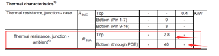
I plan to use two LM74700-Q1 to achieve ORING function, the input power is DC 18V~32V, the regular voltage is DC 24V, the current is 200A. does TI have a manual about the field tube selection method for using MOS tubes in parallel under high current? For example, if the voltage is 24V DC, the current is 200A, and the operating temperature is -40℃~85℃, how many can be driven by LM74700-Q1 to achieve the demand? 

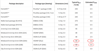
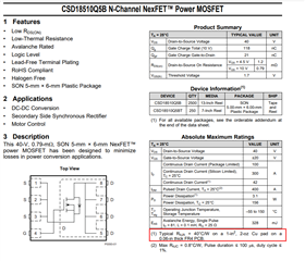
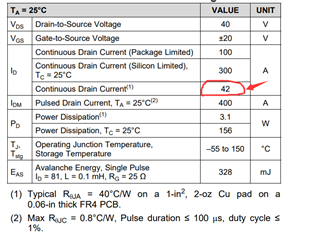
How many parallel connections should be used for the CSD19533Q5A for example?

  • Hello SHENG YANG,

    Thanks for your interest in TI FETs. TI has a load switch FET selection tool (link below) that may be used to determine how many parallel FETs are required to carry 200A continuous current. At this time, the tool does not have the capability to parallel FETs but you can divide the current by the number of FETs to estimate the power loss per FET. For this application, you will need at least a 40V FET unless there are transients that exceed 40V. In general, for the same die size/package size, a lower voltage FET will have lower on resistance than a higher voltage FET.

    I started with 5 FETs in parallel, 32V, 200A (40A per FET) and assumed a maximum operating junction temperature of 125°C. For a 40V FET, TI's lowest on resistance device in 5x6mm SON package is the CSD18510Q5B (0.96mΩ max at VGS = 10V) and the estimated power loss per FET is ~2.5W. The 5x6mm package is capable of about 3W maximum on a multilayer PCB with a good thermal layout. If you need a 60V FET, then the CSD18540Q5B is the lowest on resistance FET in the 5x6mm package but you will require at least 7 FETs in parallel (~2.7W per FET). If you need a 100V FET, then I'd recommend using a D2PAK FET such as the CSD19536KTT with at least 7 FETs in parallel.

    Link to load switch FET selection tool: https://www.ti.com/tool/LOAD-SWITCH-FET-LOSS-CALC

    Link to technical article on FET package power dissipation capability: https://e2e.ti.com/blogs_/b/powerhouse/archive/2019/10/29/selecting-the-right-power-mosfet-power-block-package-for-your-application

    Pleas review and let me know if you have any questions.

    Best Regards,

    John Wallace

    TI FET Applications

  • HI. John.

    As shown in the table below, when the power is 3W when the ambient temperature of the components can only be 30 ℃ to meet the junction temperature does not exceed 150 ℃, to CSD18510Q5B for example, the current calculated at this time is about 61 A. I understand this correctly?

    I use my design as an example, the current needs to be 200A, using the CSD18510Q5B about 5 of them. The current is 40A each and the use temperature is -40℃~85℃. According to the junction temperature calculation formula: TJ= TA + (ΘJA × P) to calculate TJ, 85 + (40 * (1600 * 0.00079)) = 126 < 150, is able to meet the requirements. In the circuit design I can choose a multilayer board and 2OZ of copper foil thickness, but about the area of the PCB used by the components may be difficult to meet. For example, ΘJA = 40 when the need for MOS tubes need to occupy an area of 1 square inch, which is a large area. If 5 MOS tubes are used, how should the area occupied be handled to meet ΘJA=40?

  • As shown in the figure below, 42A is the current at what TA temperature?

  • Hi Sheng Yang,

    Thanks for providing your calculations. Regarding the continuous drain current rating in the datasheet, the link below is to a blog that details how TI makes this calculation. For this calculation, TI uses the max on resistance (0.96mΩ) specified in the datasheet at TA = 25°C, TJ = 150°C & VGS = 10V. This calculation also takes into account the positive temperature coefficient of Rds(on) shown in Figure 8, which is a multiplier of about 1.8 at VGS = 10V and TJ = 150°C. Here is the datasheet calculation:

    PDmax = (TJmax - TA)/RθJA = (150°C - 25°C)/40°C/W = 3.125W

    IDmax = √PDmax/Rds(on)max(@TJ=150°C) = √(3.125W/(0.96mΩx1.8) = 42.5A (datasheet value is 42A)

    For TA = 85°C, the calculation becomes:

    PDmax = (TJmax - TA)/RθJA = (150°C - 85°C)/40°C/W = 1.625W

    IDmax = √PDmax/Rds(on)max(@TJ=150°C) = √(1.625W/(0.96mΩx1.8) = 30.7A

    Keep in mind, most users derate the MOSFET maximum operating junction temperature by some amount for reliability purposes. Typically, this can be anywhere from 10°C to 25°C depending on reliability requirements. This further reduces the current capability of the FET. For example, if the max operating TJ is derated by 25°C to 125°C, then at TA = 85°C, then the max current is reduced to 25.4A.

    Lastly, with a good layout on a multilayer PCB, the value of RθJA can be reduced to around 20°C/W to 25°C/W which will increase the continuous current capability. The layout of the FETs should maximize the copper for the drain pad and include thermal vias to the internal layers and bottom layer to spread the heat from the FETs. I am including a link to a TI reference design for a motor drive using the CSD18510Q5B which shows a 2 layer PCB layout with thermal vias.

    http://e2e.ti.com/blogs_/b/powerhouse/archive/2015/05/25/understanding-mosfet-data-sheets-part-3

    https://e2e.ti.com/blogs_/b/powerhouse/posts/understanding-mosfet-data-sheets-part-6-thermal-impedance

    https://www.ti.com/tool/TIDA-010251

    Best Regards,

    John

  • Thank you very much.John.

    I will study the linked material of your reply.

    Regarding the above answer, if TA = 85°C, the maximum current drops to 25.4 A. My calculation results not 25.4 A but 24.05 A. Where is the calculation incorrect? The calculation is based on the formula as follows:

    PDmax = (TJmax - TA)/RθJA = (125°C - 85°C)/40°C/W = 1W

    IDmax = √PDmax/Rds(on)max(@TJ=125°C) = √(1W/(0.96mΩx1.8) = 24.05A

    Is this calculation correct?

    As shown in the figure below, I found a MOS tube top layer with metal heat sink in Infineon's product IAUS300N08S5N012T. The RthJA of this product is divided into top and bottom layer values, how to calculate TJ when calculating? I did not find a similar product in TI's products, only the CSD88584Q5DC 40-V Half-Bridge NexFETTm Power Block.

  • Hi Sheng Yang,

    In my earlier calculation, I assumed max operating TJ = 125°C and the Rds(on) multiplier at that temperature is around 1.6 instead of 1.8. That is why the calculated current is higher.

    TI does not have any discrete FETs with topside cooling. The primary path to remove heat from the FET is thru the thermal (drain) pad on the back side of the package. For the CSD18510Q5B, RθJC(top) is about 8°C/W. Please see the blog at the link below for more information on thermal resistance. The datasheet value of RθJA is measured and includes the heat removed thru the top side of the package.

    http://e2e.ti.com/blogs_/b/powerhouse/archive/2016/06/10/understanding-mosfet-data-sheets-part-6-thermal-impedance

    Thanks,

    John

  • Hi.John.

    What is the general amount of compression of the thermal interface material after the contact between the two when the thermal interface material dissipates heat to the MOS tube?

  • Hi Sheng Yang,

    I have asked a colleague to look at the diagram and get his input on your question regarding the compression of the TIM. I'll update you as soon as I have more information.

    Best Regards,

    John

  • Hi Sheng Yang,

    I received the feedback below from my colleague. He also provided the attached example of some TIM materials from a supplier.

    From my colleague:

    The picture appears to me that the customer wants to attach the PCB with a MOSFET soldered on it
    to a heatsink with a Thermal Interface Material in between.

    Condition about the PCB :
    There must be sufficient thermal via to conduct thermal energy from the MOSFET to the
    bottom layer of the PCB and the bottom layer must has a metal plane that is plated but
    not cover by solder mask.

    The Thermal Interface Material (TIM) datasheet usually specify the minimum compression
    require to get the TIM with best performance. See attachment for example.

    If it is not in the datasheet, customer should check with the material supplier.

    Best Regards,

    John

    TIM Example.pdf

  • Thank you very much.John.