This thread has been locked.

If you have a related question, please click the "Ask a related question" button in the top right corner. The newly created question will be automatically linked to this question.

UCD90320EVM-783: Margining R3 and R4 values

Part Number: UCD90320EVM-783

Hello,

In the document SLVA845A - Design Voltage Margining Circuit for UCD90xxx Power Sequencer and System Manager it says that ideally R3 and R4 for the voltage margining circuit should be equal.

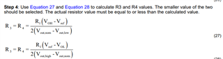
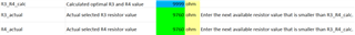
This is reiterated in the UCD90xxx Margining Circuit Design Tool.

However in the schematic for UCD90320EVM-783 schematic it shows R3 values that are significantly larger than R4

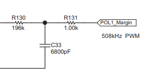
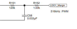
Is there a benefit to this? Can I ask why this was done?

Thanks,

Martin

  • HI

    I can not see anything other that the equation 21 that large R3 has smaller ripple.

    following the recommendation at beginning and fine tune when the board is back.

    Regards

    Yihe

  • Hi,

    Thank you for your response. Can I confirm I understand correctly? The sum of R3+R4 is the only strict requirement since this determines the margin high and low range. Making R3=R4 can be beneficial as it will allow for the lowest value of C1, and a lower C1 value minimises the startup overshoot. But if you need more C1 ripple attenuation so that it doesn't appear at the power supply output, you can make R3 larger. But if R3 is made larger then R4 must be made smaller to keep R3+R4 constant. But if you make R4 smaller then C1 must be made larger to keep the response of the R4+C1 filter the same.

    So it then becomes a trade-off between needing more ripple attenuation from a larger R3 and minimising the overshoot from a larger C1?

    Is that correct?

    Thank you,

    Martin

  • Hi

    Yes, your understanding is right.

    Regards

    yihe