The above design as per webench tool doesn't connect from SNS to ANY-OUT pins for 0.925V output.
Is it issue with the tool , please comment on this.
Original question:

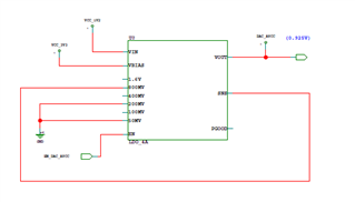
TPS7A85: configuring Output voltage by ANY-OUT Programmable pins.
The above design as per webench tool doesn't connect from SNS to ANY-OUT pins for 0.925V output.
Is it issue with the tool , please comment on this.