This thread has been locked.

If you have a related question, please click the "Ask a related question" button in the top right corner. The newly created question will be automatically linked to this question.

UCC21750QDWEVM-025: UCC21750QDWEVM-025

Part Number: UCC21750QDWEVM-025
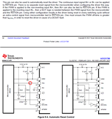
Other Parts Discussed in Thread: UCC21750, UCC21710
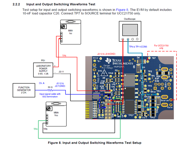
  1. Test input-output function of UCC21750 by UCC21750QDWEVM-025. Why need to link TP7 and source while UCC21710 don't have to do this?
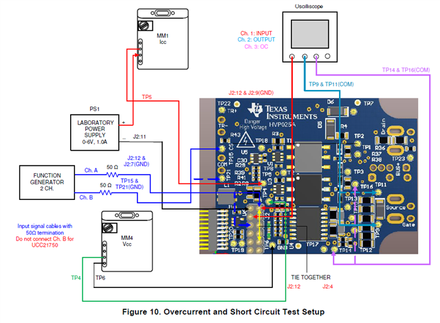
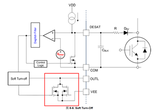
  2. Test overcurrent function for UCC21750 by UCC21750QDWEVM-025, why need to link pin IN+ and pin EN? Can you offer the detailed timing diagram?

  • Hi Brody,

    Thanks for the interesting question.

    1)

    For UCC21710, the EVM uses different test points and not TP& as shown below

    However, UCC21750 uses TP7 as shown below:

    The reason for linking TP7 to source is to short DESAT to ground and check the switching performance. 

    2)

    Please find the details below as shown in the datasheet:

    We don't have a specific timing diagram for this application. However, the timing diagram can be drawn using the explanation in the datasheet.

    Hope this helps!

    Best,

    Pratik

  • Thanks for your great help. These replies solve my problem successfully.

    Can you tell me how does it work below parallel construction of N-MOSFET? Specially, how does it to keep constant current 400mA?

  • Hi Brody,

    That structure acts like a constant pull-down current source. The transistor level design is present inside the soft-turn off block. 

    Best,

    Pratik