This thread has been locked.
If you have a related question, please click the "Ask a related question" button in the top right corner. The newly created question will be automatically linked to this question.
Hello,
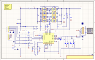
I am currently working designing a BMS using a BQ40z80. OCD is set to 5A. I am using a power supply in-place of a cell stack and a programmable load.
Everything works and trips as expected at slightly above 5A.
Increasing the load current to 10A or above causes the DSG output to transition from 27Vdc to 0V as expected, but will then come back at whatever the input voltage is.
The BMS no longer will control the DSG output.
I have attached my schematic to see if I have made any design mistakes.
So far I have lowered R10 to 4.7k and 2.2k with different results. DSG will go to 20Vdc for a few more cycles and then fail.
I have changed the discharge FET count from 4 to 2 with no change.
Any help is appreciated
.
Hello Alex,
Do you have scope captures from the test which is causing the failure? Are you still able to communicate with the gauge after the DSG pin is no longer driven high or low?
Generally with multiple parallel FETs there will be resistor going to each gate to prevent ringing on the nodes which can cause damage, are you able to add these to your design? I would also recommend increasing your PBI capacitance to 10uF for multiple FETs in parallel due to their added gate resistance the gauge needs a large burst of current to turn them on.
Sincerely,
Wyatt Keller
Hello Wyatt,
Your comments about the multiple FETs helped to point me in the right direction. Here's what I have done so far:
• I reduced the design to one pair of FETs for testing this problem.
• I changed R9 to 1k and R10 to 4.7k to more closely match the EVAL module.
• I changed C5 which is the PACK input capacitor from 100nF to 10nF to match the EVAL module. I saw a forum post for the BQ40z60 that suggested changing this capacitance to help with this problem. I'm not sure if it helped, but the value was wrong.
I have done several high current tests with results as expected with one pair of FETs. I plan to gradually add more pairs and increase the supporting circuitry and try to get to 4 pairs.
I do have a few more questions:
• What values do you suggest for the DSG/CHG output resistors and the the FET gate resistors?
• The CHG and DSG FETs are working separately during the corresponding safety event. Is there a setting that will make both FETs turn off at the same time during any safety event?
Hello Alex,
Glad you are getting it closer to working as desired.
The resistors are dependent on multiple factors, mostly how fast you need the FETs to turn on and off and how much ringing the system can tolerate.
The CHG and DSG FETs are in series, each protection will disable the corresponding FET, like OCD disables the DSG FET. If you disable both FETs there is no path for recovery since they thresholds are normally based around current. I'm not sure why you would need both FETs off for the protections.
Sincerely,
Wyatt Keller
Hello Wyatt,
Here is my final fix for this problem in-case anyone else has the same issue.
For my application, I changed the DSG resistor to 2.2kΩ and added 100Ω resistors to each discharge FET gate.
This fixed all of my discharge issues.