This thread has been locked.

If you have a related question, please click the "Ask a related question" button in the top right corner. The newly created question will be automatically linked to this question.

LM51561: Power Supply unable to handle load it is designed for

Part Number: LM51561

I'm having issues with this boost supply in two different instances

Issue #1:

Input is 3.5V to 4.2V

Output is 18V, with an expected load of 500mA

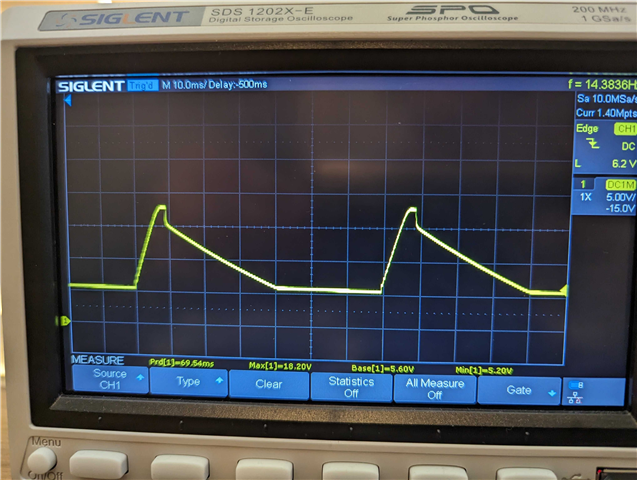
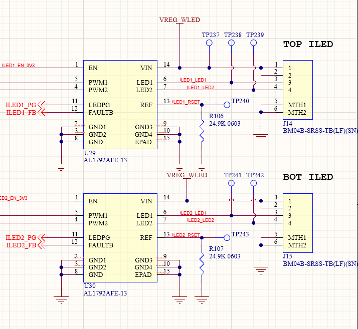
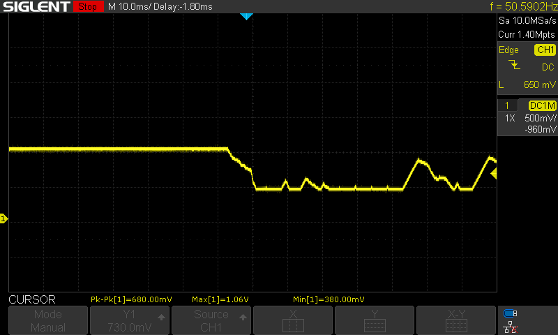
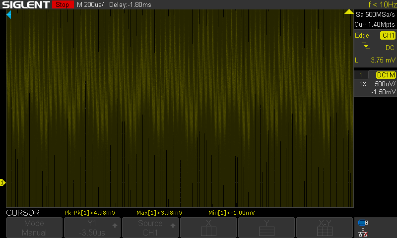
This power supply provides power to two LED light bars, with two channels each.  Each channel is 120mA for a total of 480mA.   I designed the circuit with a little extra buffer at 750mA.  The LED light bars are driven by a current sink (AL1792AFE-13 by Diodes, Inc) set to 120mA per channel.  When both light bars are turned on, they start to flicker and I see that the voltage rail collapses.  Here is the link to the simulation.  Below you can see a scope shot of the rail collapsing

https://drive.google.com/file/d/15bhAi8sB0FTvUNNfBODUVxSrG4kT-2Vg/view?usp=sharing

I'm also including a snippet of the circuit
Note: R156 is installed, PS_SYNC_3 is not present, and R158 has been changed to 9mOhm 1W per Webench recommendation.

https://drive.google.com/file/d/1_1B_9mfgefExwVK4zpFzaSLLeeAZnzoG/view?usp=sharing

https://drive.google.com/file/d/14d6bEUGmVTZCIQaIC-4G4rdiCealhirj/view?usp=sharing

I have used a benchtop supply to look at what the exact load from the LEDs are.  The load does not exceed 540mA.  I've played around with the design in webench and changed components to try and match the eval kit.  This does yield in good results.  The question remains though, why is the power supply which is designed for 750mA not able to handle a constant current load of 540mA?

Issue #2:

Input 3.5V to 4.2V

Output 16V, expected load of 630mA, designed for 750mA

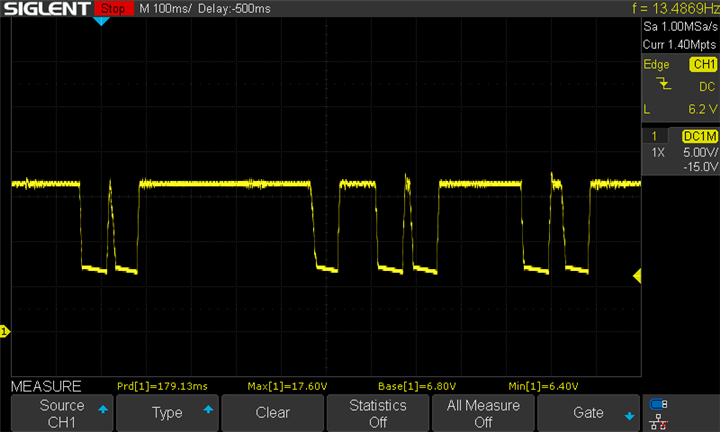
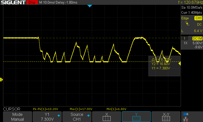
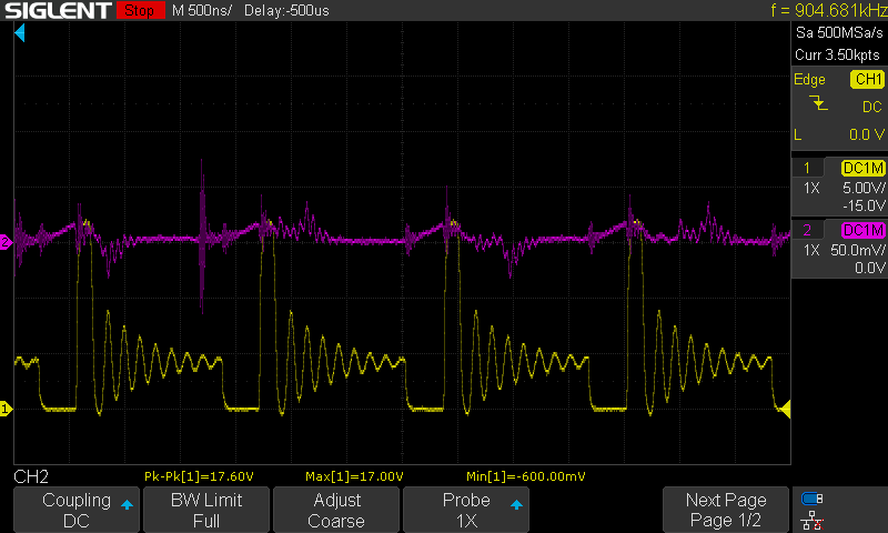
This 16V rail goes on to power and amplifier for audio playback.  At full volume, the audio starts to clip and I can see that the voltage rail collapses by 10V or more.  See scope shot below:

https://drive.google.com/file/d/15uczyq0s-Xgx8rrUAuBy4mJqFjVBcSX-/view?usp=sharing
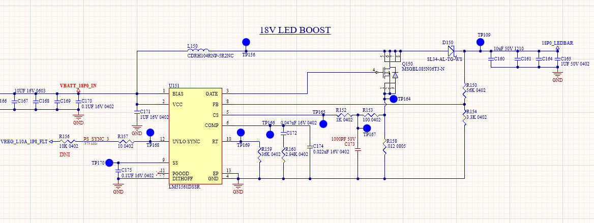
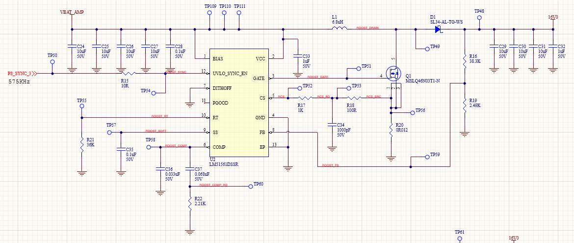
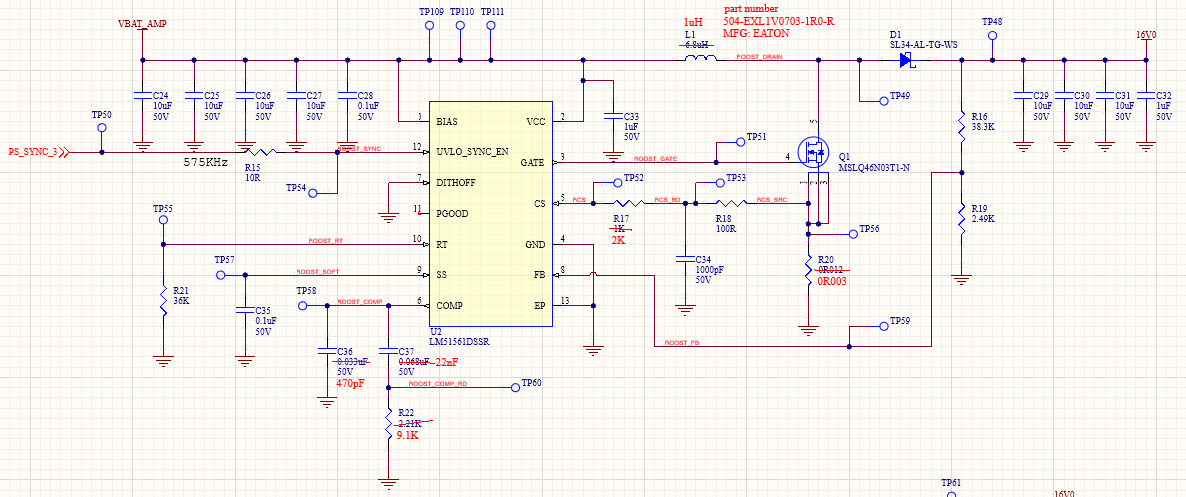
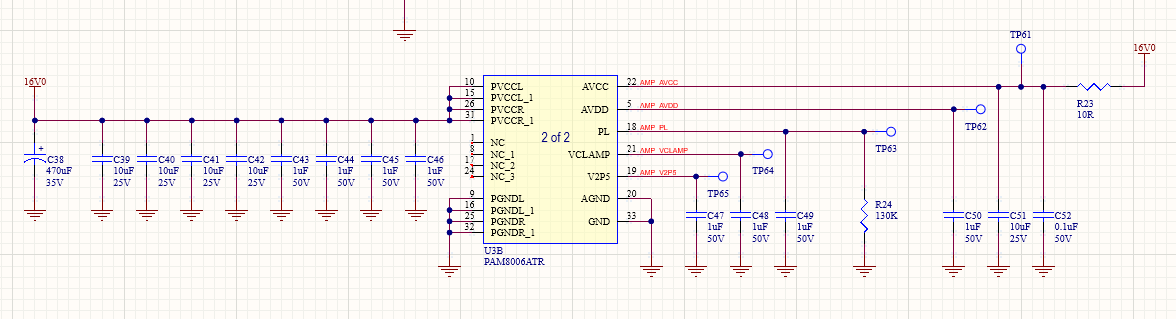
Schematic:

drive.google.com/.../view

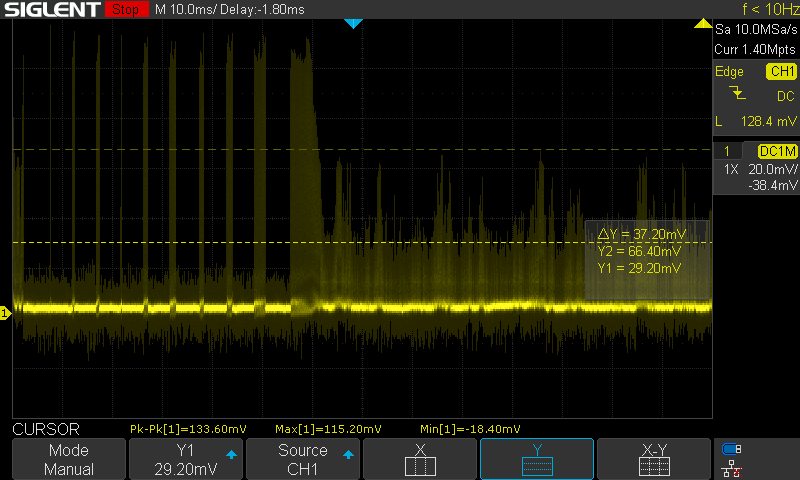
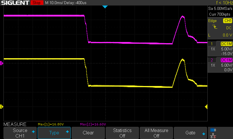
It turned out that there was some transient current of about 2A.  I redesigned the supply to accommodate for this.  The audio clipping is gone at full volume but I still see the rail collapse.

https://drive.google.com/file/d/1tGlATTDgEAlgP7x7d9vboZcmjt0KBpSP/view?usp=sharing

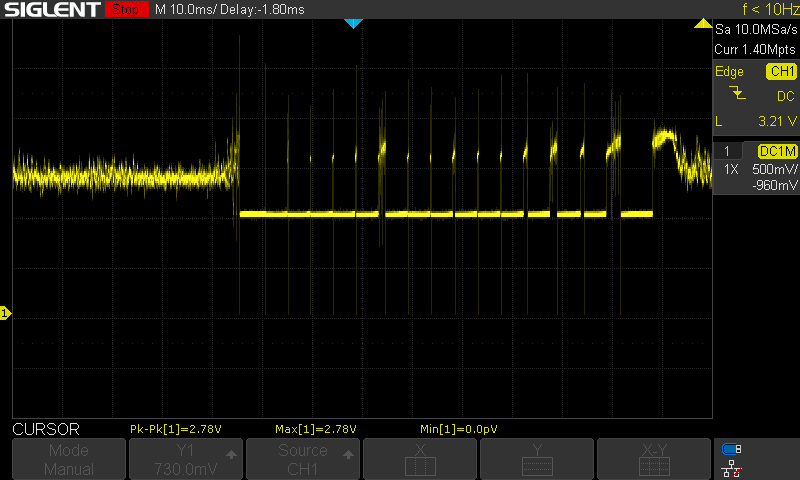
As an experiment, I spliced in the eval kit and still saw voltage rail collapse similar as shown above.  I went ahead and spliced in a benchtop power supply as well and that did not exhibit any voltage rail collapse.  Although the audio playback clipping is gone, seeing the rail collapse is concerning.

  • Hello Omair,
    Thanks for reaching out to us via e2e.

    I cannot really access the material you have provided. Anyway, I am trying to answer.

    But I also have some questions.

    Case 1 (LED light bars).

    Do I understand correctly that you are initially starting the booster with no load?
    Then, suddenly you turn on the Light bars (maybe together or one after the other).
    But in any case you are causing an immediate change of the output current.
    Is that correct?

    Instead of "playing around with the design in Webbench", please use the Quickstart Calculator tool to calculate the external components and the compensation network.
    You can download it from here: www.ti.com/.../SNVC224

    I am sorry, I cannot download the schematic, so I cannot compare the results.
    The calculator would give me 3.3µH for the inductor and if I follow that, I get about 10mOhm for the sense resistor.
    But the required sense resistor value changes, dependent on the chosen inductor!

    A 10mOhm sense resistor will set the peak current limit to 10A.
    So, the saturation current of your inductor must be much higher than 10A.
    Also, your bench supply must be able to deliver more than 10A without clipping.

    It looks like you are running into some kind of overload condition.
    Maybe your inductor is going into saturation or your power supply has a current limit that is not high enough.
    There are also other things that could happen (e.g. a voltage drop on the cable is triggering the UVLO).
    Which UVLO voltage did you configure?

    The Quickstart calculator will also help you to simulate the compensation.
    But the real components will need to be determined in experiments to minimize over- / undershoots.

    So, as a first step I would ask you to use the Quickstart calculator and fill in all the data, then you will get a better understanding which of your components are off.


    Case 2 (Audio amplifier)

    An Audio amplifier is a highly dynamic load.
    It is not the usual case that you would expect the booster to quickly follow these changes.
    Instead, you will need to implement a big buffer between booster and amplifier, from where the amplifier can draw the peak power that is required.
    On some of our prototypes or reference designs we have even implemented up to 3000µF (!) as a buffer capacitance.
    So, the booster will basically need to supply the average power plus some little overhead.

    Best regards
    Harry

  • Thank you for the feedback, Henry. 

    Case 1:

    But in any case you are causing an immediate change of the output current.

    Yes that is the correct assumption. I will look at the quickstart calculator and adjust the design accordingly.

    The calculator would give me 3.3µH for the inductor and if I follow that, I get about 10mOhm for the sense resistor.

    Looks like there's a difference between what Webench recommends vs. Quickstart Calculator.  I assume Quickstart Calculator to be the more accurate of the two.  I'm being shown 5.6uH and 9mOhm resistor.  Same as above, I will run the numbers through Quickstart Calculator.

    Which UVLO voltage did you configure?

    I'm not using UVLO.  In our final design we will have an external sync clock on that pin (575kHz).  For my prototype I have that pin pulled up to 1.8V with a 10K resistor.

    Case 2 

    Once again, I will use the quickstart calculator to see what kind of output capcitance is needed.  We currently have 540uF of total capacitance.  The largest cap is 470uF which was intended to to be the buffer but may not be large enough.

    I was having trouble uploading the images yesterday so I'll try again below.  Hope they come through:

    Issue #1:

    Below you can see a scope shot of the rail collapsing

    /resized-image/__size/320x240/__key/communityserver-discussions-components-files/196/8233.image-_2800_15_2900_.png

    I'm also including a snippet of the circuit
    Note: R156 is installed, PS_SYNC_3 is not present, and R158 has been changed to 9mOhm 1W per Webench recommendation.
    Issue #2:
    Scope shot:
    Schematics
  • Hello Omair,

    Correct, the Quickstart calculator is more accurate.
    I can see the images now, but the resolution (320x240) is very small, so when I zoom in, I cannot read the schematics.
    Can you please try again with a better resolution,

    Thanks and regards,
    Harry

  • Let's try the images again

    Issue #1:

    Below you can see a scope shot of the rail collapsing

    I'm also including a snippet of the circuit

    Note: R156 is installed, PS_SYNC_3 is not present, and R158 has been changed to 9mOhm 1W per Webench recommendation.

    Issue #2:
    Scope shot:
    Schematics

    Last note, I did experiment with increasing the capacitance by adding another 470uF but no improvement was observed.

  • Hello Omair,
    Thanks for uploading the images again. I can read them now.
    I will look into your problem and come back to you at the mid of the week.

    Best regards,
    Harry

  • Hello Omair,

    I reviewed the schematics for both of your applications and it seems, that in both cases the phase margin of the closed loop is very low.

    This can lead to an unstable loop. I recommend to first adjust the components of the compensation network according to the recommendations of the quickstart calculator. The phase margin should be around 60 degrees.

    Best regards,

    Moritz

  • Do you know what the maximum output current supported by this device is?  I did not see any mention of Iout in the datasheet

  • For the 16V audio amplifier circuit, I used the quick start spreadsheet (attached) and populated the following components.  Similar to before, the symptom of the audio clipping at full volume  seems to be resolved but I'm still seeing a voltage drop of about 9.3V on the rail.  Though it seemingly has no affect on the user experience, will this have any long term affects on the electronics?

    16V Amp.xlsx

    Components used:

    Inductor
    https://www.mouser.com/ProductDetail/504-EXL1V0703-1R0-R

    Rs
    https://www.mouser.com/ProductDetail/KOA-Speer/TLR2ATTD3L00F?qs=7zIQ0yXu9nMdcEf2Ujwx1A%3D%3D

    Rcomp
    https://www.mouser.com/ProductDetail/667-ERJ-UP3F5101V

    Ccomp
    https://www.mouser.com/ProductDetail/791-0603B223K500CT

    Chf
    https://www.mouser.com/ProductDetail/791-0603B152K500CT

  • Hi Omair,

    The maximum current depends on the external parts that are used, like MOSFET, Diode,Inductor..

    I see in the attached spreadsheet you used a maximum output current of 5.1A? So in this case you might trigger the overcurrent limit.

    Can you please attach waveforms of the voltage at CS-pin? And please also add waveforms of FB pin and COMP pin.

    Best regards,

    Moritz

  • Hi,

    The reason I set the current to 5.1A is because when I use my benchtop power supply to inject the16V instead of using the boost supply, I don't run into the issues we've been discussing.

    Please see waveforms as requested:

    CS:

    COMP

    FB:

    Please also see specs for MOSFET and Diode

    MOSFET:

    2251.MOSFET.pdf

    Diode:

  • Hi Omair,

    Thanks for the scopeshots. Is the selected slope compensation resistor 2.1k as used in the calculator or 1k according to the schematic? Also the output capacitance and the feedback divider have different values in the spreadsheet compared to the schematic. However, these values will affect the gain and the phase.

    The controller might hit current limit, but can you please send a more zoomed in waveform of CS-pin? Also the RC-Filter at current sense (R18, C34) seems to big for the switching frequency. You can try to reduce C34.

    Best regards,

    Moritz

  • Hi,

    Please see zoomed in shots of the CS pin.  I took a few different ones.

    I updated the feedback resistors which resulted in having to change Rcomp, Ccomp, and Chf.  I'm attaching an updated spreadsheet with all of the passives being used.

    I changed C34 from 1000pF to 470pF as well.

    The changes above resulted in the audio clipping symptom to return.

    16V Amp_v02.xlsx

  • Hi Omair,

    From your spreadsheet it seems that your peak inductor current is 28A and the current limit is set to 18.6A, I think you are hitting the overcurrent limit as you go full load, at what load do you see this issue presenting itself?

    BR,

    Haroon

  • Hi Haroon,

    I see this issue at 75% to 100% load.

    The expected load is 750mA with transients up to 4A.

  • Hi Omair,

    I see the output current as 5.1A, so how is it 750mA?

    BR,

    Haroon

  • Haroon,

    Some background as to why I set it to 5.1A.

    This boost supply is intended to supply power to an audio amplifier.  The design dictates that the amp will draw 650mA at 16V with full load.  We designed it to 750mA to add some buffer.  What we saw at full load was the audio playback was clipping and that the voltage rail was collapsing (you can see the scope shots in the posts above.

    The only way I got the amplifier to work correctly was by injecting 16V with a benchtop power supply with the current limited set to its max of 5.1A.  There must have been transients higher than what I was measuring on my scope and that's why I went with 5.1A, as that was the current limit that worked.

    The original design of 750mA at 16V does not work.

  • Hi Omair,

    I see, ok could you do me a favor and have a waveform of output load, SW node, CS and Vout in one image? right now the problem you are facing is the voltage rail collapsing, correct?

    BR,

    Haroon

  • Hi Haroon,

    Please see attached scope shots.  Unfortunately I don't have a 4 channel scope so I took 2 captures at a time.  The first one is SW node on CH1 measured at TP49 and CS pin on CH2 measured at TP52. 

    The ringing you see on the SW node exists even when there is no audio playing, meaning it has minimal load.  The scope shots were taken at full load

    The second scope shot below is Vout on CH1 measured at the cathode of D1 and Vload on CH1 captured at C41, which was the closest point to measure near the amplifier.

  • Hi Omair,

    I am very confused, I think you send out multiple Schematics and none of them matches the spreadsheet you have attached. Could you please check your excel sheet, it has wrong inductance and Rsense values, it is confusing. Could you please just keep one schematic file as pdf and one excel sheet instead of multiple ones.

    BR,

    Haroon

  • Hi Haroon,

    Since I'm changing components on my circuit board I am not updating the schematic.  The schematic that I originally attached is how the circuit was designed.  Since then I have been making incremental changes by swapping out components such as inductors, resistors and capacitors.  We were initially dealing with two separate issues.  Issue #1 was related to driving LED's which is resolved for the moment.  We have now been working on Issue #2, which is the audio amplifier.

    Below, I will post a modified schematic of the power supply circuit with components that have been changed based on the last Quickstart spreadsheet I posted.  Hopefully that will provide you with a clearer picture.  I will also post a schematic of the circuit for the amplifer.

    Power Supply Circuit:

    Audio Amplifier Circuit (load)

  • Hi Omair,

    Thank you for the clarification, so the schematics seems ok to me. My only concern would be for audio amplifier application you would need quite some output capacitance, especially at full volume, is it possible to increase that a bit? Since i see your output voltage collapsing as you have shown in one of the waveforms in your previous message, I think it could be due to this?

    Also, why is there ringing on your SW node, could it be a layout issue? are the capacitors placed close to the IC?

    BR,

    Haroon

  • Haroon,

    Yes, I had increased the capacitance to almost triple what is shown in the design and it did not make any difference.

    I will look into why I have ringing.  I want to make sure it wasn't introduce after swapping components so I will scope it on a board with the original design.

  • Hi Omair,

    Since the schematics seems ok, I would like to see the layout and see if there is any issues there? 

    As one final thing to make sure it is not a UVLO lockout, could you also share your Vin signal alongside the Vout? I want to see what happens on Vin when the Vout collapses.

    BR,

    Haroon