Because of the holidays, TI E2E™ design support forum responses will be delayed from Dec. 25 through Jan. 2. Thank you for your patience.

This thread has been locked.

If you have a related question, please click the "Ask a related question" button in the top right corner. The newly created question will be automatically linked to this question.

LMG1020: LMG1210 PSpice Transient Model (Rev.C) does not work with cadence simulator

Part Number: LMG1020
Other Parts Discussed in Thread: LMG1210, LMG1205, LM5113, LM5114

Hello, TI experts,

I tried to simulate a power converter circuit with real TI LMG1210 gate driver pspice model in cadence virtuoso environment. 

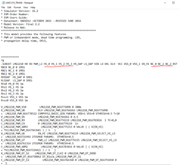
Saw this error when I imported it in as spice model. 

I also tried with LMG1205, still not luck. But, I remember the LM5113 and LM5114 pspice model works before in cadence, and also remembered all the models works with LTSPICE.  Attached the models (neither of them works). 

Could you guide me how to fix the model that it will work with cadence tools? 

Thanks,

LMG1210_TRANS.liblmg1210.lib

  • Hey Hua,

    Thank you for your question regarding the LMG1210.

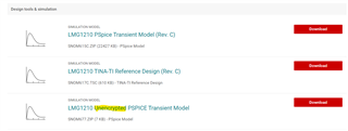
    Are you using the unencrypted PSPICE model? You can find it on the product page at this link. It will be in the Design & Development Section and look like this:

    Let me know if this doesn't solve your problem or if you have further questions.

    Thank you,

    William Moore

  • Still no luck!

    Just double checked one more time. I am using the unencrypted PSPICE model. it does not work(Same error message likes the previous one).

    More information, I also tried the same circuit and spice file with LTSPICE. the simulation run through. I saw waveforms, but I saw one expected voltage spikes occurring every 20-30 periods. Attached one LTSPICE error message (two pictures).

    thanks and let me know any comments.

  • Hi Hua,

    I recommend you check out these threads:

    https://e2e.ti.com/support/power-management-group/power-management/f/power-management-forum/952799/lmg1210-getting-error-in-ltspice-while-using-unencrypted-pspice-model

    https://e2e.ti.com/support/power-management-group/power-management/f/power-management-forum/1004807/lmg1210-lmg1210-working-ltspice-model-with-no-errors

    Usually, a PSpice model and LTspice model can be used interchangeably. However, there are some functions supported in one and not the other. The LMG1210 model uses some of those so it doesn't work perfectly in LTspice. In the second thread, this person claims to have made one that works in LTspice, but I have never verified it and it is coming from a stranger. 

    Also, watch out for the HS_DAP pin. I think it is connected to GND in the model, not HS.

    Thanks,

    Alex M.

  • Alex or Other TI Experts,

    I have a few more questions still related with TI LMG1210 official unencrypted PSPICE model. 

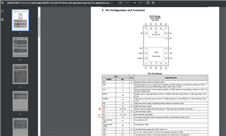
    1. I found 4 NC pins+ 3 HS pins in LMG1210 rev D datasheet vs. found 3 NC pins +4 HS pins in PSPICE model. Can you help with the wiring connections? where to where? (HS_0 HS_1 HS_2 _HS_3 VCC NC_0 NC_1 NC_2 HS_DAP LS DAP)

    2. I assume the Thermal Pad(HS) is HS_DAP, thermal pad(LS) is LS_DAP. I wired both to gnd. If my HS pins connect to a voltage for example, 36V-24V(low side is not Zero), I guess HS_DAP should still connect to gnd. am I right? 

    3. I bet vcc =vdd =5V, if my circuit is not similar to half bridge. (for example like a three level buck or DSD), HS pins is not switching between VIN=36V and GND. will this chip work for Vin higher than 18V? (because the Vin in the datasheet says 6-18V.) Or, can I tried to break the BST pin, disabled the VIN. connect high Vin(>=36V) to positive term of diode? 

    Thanks

  • Hi Hua,

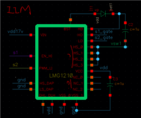
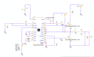
    Here is my simulation schematic that is currently working in PSpice for TI:

    I connected all of the NC pins to GND, and HS_Dap is connected GND via a 1pF capacitor. It actually can be connected directly to GND, but HS_dap should be connected to HS in an actual system. This is just an issue with the model. 

    1. I found 4 NC pins+ 3 HS pins in LMG1210 rev D datasheet vs. found 3 NC pins +4 HS pins in PSPICE model. Can you help with the wiring connections? where to where? (HS_0 HS_1 HS_2 _HS_3 VCC NC_0 NC_1 NC_2 HS_DAP LS DAP)

    If you just ground the NC pins your schematic, it looks like it will match mine. Again, I would follow the datasheet in the actual system (NC1 floating or HS), but its fine to tie it to ground in the simulation. 

    2. I assume the Thermal Pad(HS) is HS_DAP, thermal pad(LS) is LS_DAP. I wired both to gnd. If my HS pins connect to a voltage for example, 36V-24V(low side is not Zero), I guess HS_DAP should still connect to gnd. am I right? 

    HS_DAP is the high-side thermal pad, and should be connected to HS in the actual system, which can be about -300V to 300V with respect to GND. 

    3. I bet vcc =vdd =5V, if my circuit is not similar to half bridge. (for example like a three level buck or DSD), HS pins is not switching between VIN=36V and GND. will this chip work for Vin higher than 18V? (because the Vin in the datasheet says 6-18V.) Or, can I tried to break the BST pin, disabled the VIN. connect high Vin(>=36V) to positive term of diode? 

    I don't think I have seen anybody use this IC in a multilevel topology. The important thing to note is that Vin is rated with respect to GND and not HS. If either Vin or VDD exceed their absmax rating, there is a potential for damage to the IC. I am having a hard time following the verbal description of the circuit, so I'm not sure if what you are proposing will work. 

    As long as your solution maintains 5V across VHB - VHS and 5V from VDD-GND, and follows the other limits in the absmax table, it should work. 

    Thanks,

    Alex M.