


Avalanche breakdown in power FETs
Avalanche breakdown can occur in any power FET, as its preconditions are met when the FET is off and there is a high potential from drain to source. It is an important design consideration for systems exposed to high voltage and subject to rigid safety requirements, since the destructiveness of avalanche breakdown can compromise a power FET. This FAQ reviews avalanche breakdown, its effects, and important design considerations.
What is avalanche breakdown?
Avalanche breakdown is a form of electron mobilization that occurs when a light to moderately doped p-n junction is heavily reverse biased. In a FET, this is a strong drain-to-source voltage reverse biasing the body diode, or the junction between the p and n- layers. When the electric field is strengthened beyond the critical electric breakdown field, a threshold intrinsic to the silicon, a small number of electrons mobilize and pass through the junction.

Figure 1. I-V curve of the p-n junction
The field accelerates the electrons, giving them considerable kinetic energy where upon collision with the crystal lattice structure, their energy excites other valence electrons and destroys their covalent bonds. The newly free electrons similarly accelerate, collide, and dislodge others, creating the avalanche. Figure 2 shows a cross-section of a MOSFET and a close view of the avalanche at the p-n junction.
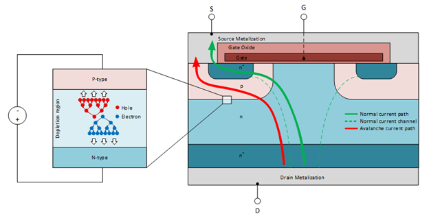
Figure 2. Cross-section of a vertical MOSFET during avalanche breakdown
Effects of avalanche breakdown in a system
Avalanche breakdown occurs when the FET is exposed to a voltage that exceeds its breakdown voltage. Figure 3 provides an illustration of this. Both FETs are in an OFF state with a breakdown voltage of 1300V. In the diagram on the left, there is no current since the input voltage of 800 V is less than the breakdown voltage. In the diagram on the right however, the input voltage is 3.5kV which causes the FET to breakdown and starts conducting current.
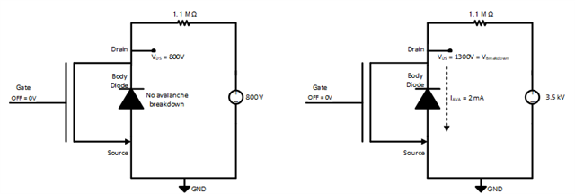
Figure 3. Avalanche breakdown at the FET's perspective
Though it is a small amount of current at the start, the high resistance causes the junction temperature to rise from the power dissipation. If the avalanche current persists, the junction temperature can rise beyond safe levels and cause irreversible damage to the FET. Luckily, there are design mitigations and technology available that can help with avalanche design and reduce the risk of damage during avalanche breakdown.
Testing for avalanche robustness
The robustness of a design against avalanche breakdown is many times revealed in High Potential Testing (HiPot), also known as Dielectric Withstand Testing. This test exposes a system to extreme voltages to confirm electrical insulation. Figure 4 shows how a HiPot test is typically administered and how tolerant the TPSI2140-Q1 and typical opto-switch solutions are of the avalanche current. TPSI2140-Q1 is the most robust against avalanche at 2 mA of tolerance, whereas a handful of opto-switch devices reach 0.6 mA.
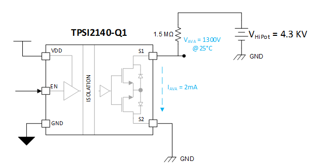
Figure 4. TPSI2140-Q1 under a 4.3 kV HiPot test
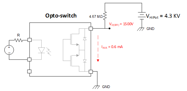
Figure 5. Opto-switch under a 4.3 kV HiPot test
A resistor is placed in series with the device in the HiPot test to reduce the power dissipation in the switch. The voltages VAVA and VO(OFF) represent the thresholds where avalanche breakdown is a concern. In opto-switch solutions, more resistors are needed to reduce avalanche current seen by the switch, adding to the cost of the BOM and increasing the size of the board. Many opto-switch solutions cannot handle any avalanche current so to prevent it entirely, designers will disconnect the circuit with a mechanical switch as shown in figure 6.
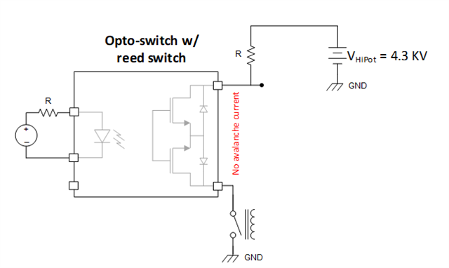
Figure 6. Reed switch implementation
Typically, a reed switch is used here, but this implementation is expensive and it experiences wear over its lifetime, reducing reliability. In simple terms, lower avalanche robustness increases the size of the BOM and board, and requires less reliable implementation.
Layout considerations for avalanche breakdown
The primary concern of avalanche current is the junction temperature overheating. This can be addressed in two ways: first, through thermal mindfulness in the design of the PCB and second, through a reduction of the avalanche current. Using TPSI2140-Q1 as an example, figure 7 shows thermal optimization by maximizing heat sinking underneath and adjacent to the FET junctions with a floating plane. Because there is no need for a bulky mechanical switch there is more space, thus more flexibility in placing the floating plane. In multilayer PCBs, floating planes can be stacked to increase thermal relief.
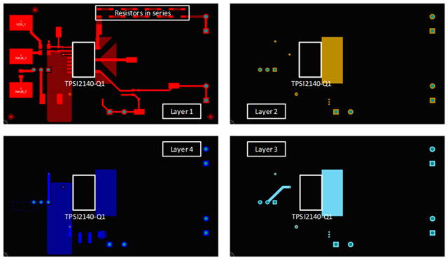
Figure 7. 4-Layer PCB with thermal relief on every layer
To limit avalanche current, resistors can be added in series with the device. These resistors reduce the current the FET sees and bear a portion of the power dissipation. This is not a simple remedy to implement, though. In battery insulation monitoring applications, too much resistance diminishes the monitoring accuracy. Therefore, it is important to start your design with devices that have high avalanche robustness.
Conclusion
Avalanche breakdown is a phenomenon where electrons accelerate under a strong electric field, causing a FET to conduct current in the OFF state. It can damage a FET from the heat it produces and is an important design factor to consider, especially as automotive electrification moves towards higher battery voltages. Devices in high voltage designs, such as insulation monitoring in an electric vehicle’s battery management system, need to have high avalanche ruggedness and ample heat-sinking if they are meant to experience the voltage directly. Conveniently, TPSI2140-Q1 provides protection from avalanche breakdown while aligning with the common design goals of reducing costs and board size and increasing reliability. The advantage of TPSI2140-Q1 is its integrated avalanche current protection up to 2 mA in a small package, allowing it to replace mechanical switches, saving costs and space.
