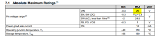
This thread has been locked.

If you have a related question, please click the "Ask a related question" button in the top right corner. The newly created question will be automatically linked to this question.

TPS62170: Damage on high VIN input

Part Number: TPS62170

Hi,

we are implementing the TPS62170 DC-DC converter in our solution which is meant to be battery-powered with an input voltage of up to 16.8V maximum (4S batteries).

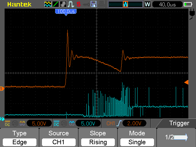
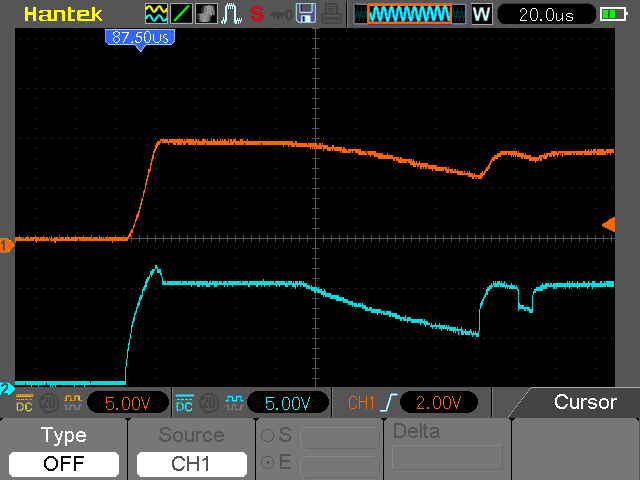
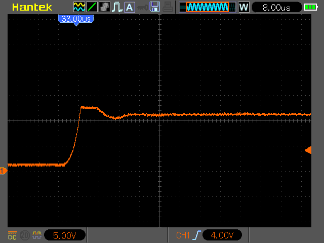
We are experiencing an issue where in a significant amount of cases (double-digit percentages) the TPS62170 gets violently damaged in <1s after connecting the VIN. In some cases there is an audible pop and a small amount of magic smoke, in other cases, the TPS62170 has caught fire. At lower voltages (~5V VIN) the device operates just fine.

The components we have selected are as follows:

C7 CAP(VIN) PN: CL10A106MA8NRNC (0603, 10uF, 25V)
L2 IND(SW) PN: MBKK1608T2R2M (0603, 2.2uH, Isat 0.52A)
C3 CAP(VOUT) PN: CL10A106MA8NRNC (0603, 10uF, 25V)
The output is regulated at ~3.3V with 470k and 150k resistors.
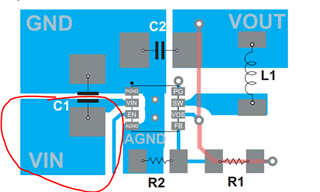
Schematic:

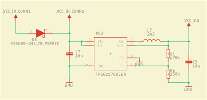
Note: The device has 2 connectors and the D6 diode separates the power rails so the connector2 cannot put voltage to the battery connected to connector1

Board layout:

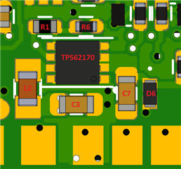
Note: We are using copper-capped vias so there are no physical holes through the PCB.

VIN copper traces on top and bottom layers:

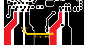
I've read similar topics I found here on the TI forum and I assume we have an issue with VIN stability due to the combination of the CAP(VIN) and the inductance caused by the PCB traces, the connector, and the battery wires. Can you please provide your insight into this assumption? But more importantly, do you have any suggestions for us on how to prevent this issue? We are actively investigating the issue on our end, however, any guidance you could offer on what aspects we should focus on and what specific measurements we should take would be immensely helpful.

Thank you for your assistance in helping us resolve this issue.

Best regards,

Michal Sebesta

  • Hi Michal,

    Yes, you're right. The damage is very likely caused by the VIN/SW pin over voltage. You can find the maximum input voltage in the datasheet is 20V. 

    However, as the rated input voltage of this device is 17V, using 16.8V input do has risk since there's no margin at all. 

    When we used a high input voltage as 16.8V, the voltage of SW to GND may have large ringing and exceed the limitation and cause the critical damage. The most possible first damage part is the low-side MOSFET. You can try to capture the waveform of SW and see the ringing when high-side FET on using the full bandwidth probe.

    The ringing is related to the input parasitic inductance and the input capacitance. 

    To reduce the ringing, we usually have below methods.

    1. Optimize the layout.

    The input trace from D6 to VIN pin is too long and too thin, this may cause large parasitic inductance. Parallel wiring over long distances as well as narrow traces should be avoided.

    We recommend to use an input copper and the input capacitance should be placed as close as possible to the IC pins.

    2. Change a larger input capacitor. 0603 10uF 25V cap may have -80% derating, the higher the input voltage, the lower the input capacitance. Maybe a 0805 cap would be better.

    3. If the ringing spike is too high, you can try to add a RC snubber between SW and PGND to reduce it.

    Please let me know if you have further questions.

  • Hi Athos,

    sorry for late reply. We did some measurements and my colleague is preparing some screenshots so I can post them here. We will optimize the layout and put a 0805 cap as you suggest.

    While brainstorming this issue, we came up with an idea of using TVS diode, is this valid option based on your experience? I understand the diode brakedown voltage will probably always be above 20 V (absolute maximum for the TPS) to achieve clamping voltage >17V of 4S battery. Even though the absolute maximum rating would be exceeded, it should prevent the spikes what we see now, when during the ringing there is up to double the VIN momentarily? Are we missing something or is this also somewhat valid option how to deal with the issue? And as a extra bonus we would get better ESD protection on VIN rail

    Thank you for your support and have a nice day!

  • Hi Michal,

    I seldom see solution using a TVS. RC snubber between SW and GND may be an common solution.

    However, with such high input voltage 16.8V, is it possible you change the device into one with 28V input ABS? Maybe it's difficult to optimize the spike below 20V.

  • Hi Athos,
    I am Michal's colleague.
    Thank you for your advice.
    I did some measurements and I want to share some results:

    Spark when switching on the power supply with a mechanical switch - power connector (VCC IN CONN2).
    Orange VIN, Blue SW


    Spark when switching on the power supply with a mechanical switch - power connector (VCC IN CONN1).
    Orange VIN, Blue VCC IN CONN1


    So in our case, the problem is overvoltage on the VIN caused by arcing. The diode in the path separates C from the power supply wires and "no oscillation" occurs. And overshoot is reduced.


    Spark on VIN, but reduced with TVS:


    So in the next revision of the device design there are diodes in the path of both connectors, then a chipbead or resistor, followed by a TVS or zener diode and then a capacitor(now 0805) with TPS...

    On the SW side, I did not make any adjustments because I did not see any problem on the oscilloscope - the peaks did not exceed the VIN.

    Just for the record.I have repeatedly tested that by slowly increasing the voltage, the TPS62170 is able to operate even at 30V. At 30.2V it goes to silicon hell.

    What kills it reliably when powered from the battery (16.8V) is just the overvoltage caused by arcing when connecting the battery - the voltage reaches up to twice what is on the input.

    I will test whether ferrite+tvs or resistor+zener diode, or just rezistor will be better to eliminate overvoltage.

    So currently, thanks for the advice, hopefully our problem will go away with the next revision of our design.

  • Hi Marek,

    Athos will give you reply once the CN holiday ends in 7th October.

    BRs

    Zixu

  • Hi Marek,

    Nice findings.

    Regarding the maximum input voltage, some parts may be able to operate under even 30V but the performance of voltage larger than ABS 20V condition is not guaranteed by TI.

    Please let me know if you have further questions.