This thread has been locked.

If you have a related question, please click the "Ask a related question" button in the top right corner. The newly created question will be automatically linked to this question.

LM61495RPHEVM: Vin-SW & SW-GND waveform behavior

Part Number: LM61495RPHEVM
Other Parts Discussed in Thread: LM61495,

I have some question on phase node measurement, so need TI clarification. As figure 1, this is schematic for 12V->5V power application. I’d like to check about Vin-SW and SW-GND voltage level.

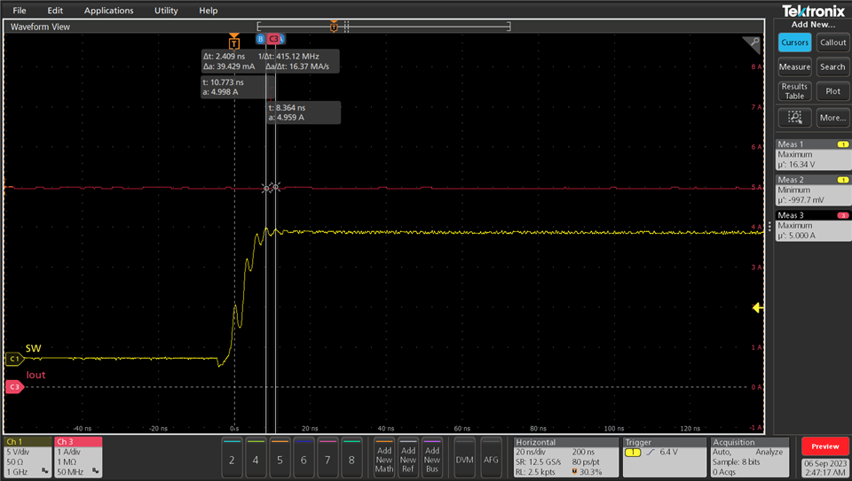
1. In general, the voltage of SW-GND (figure 3) should be higher than Vin-SW(figure 2) with loading. But LM61495 shows different result. Can you help check this result is ok?   

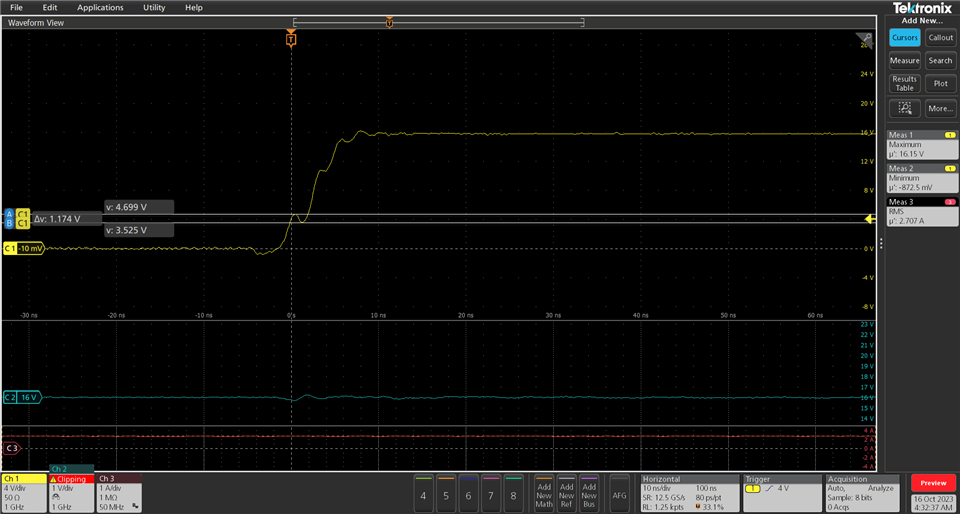
2. Zoom in the rising edge of SW-GND, some of ringing can be observed(figure 4). Is it ok for this phenomenon? What does the reason cause this phenomenon? Thank you.

  • Figure 1

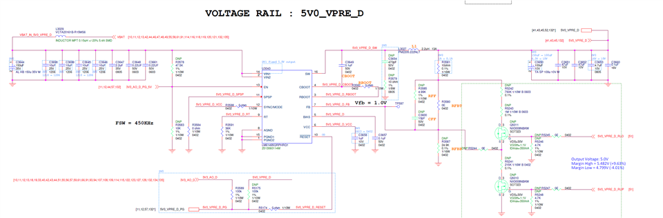
Figure 2. Vin-SW at 5A loading (please ignore meas4 date) 

Vmax=18.31V, Vmin=-0.424V

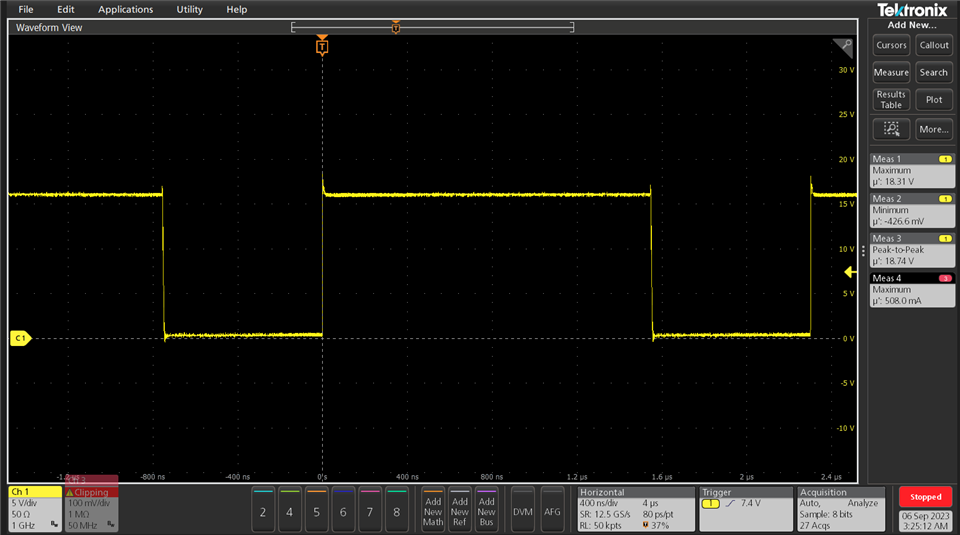
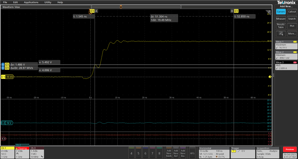
Figure 3. SW-GND at 5A loading

Vmax=16.61V, Vmin=-1.873V (Is this value ok for negative voltage)

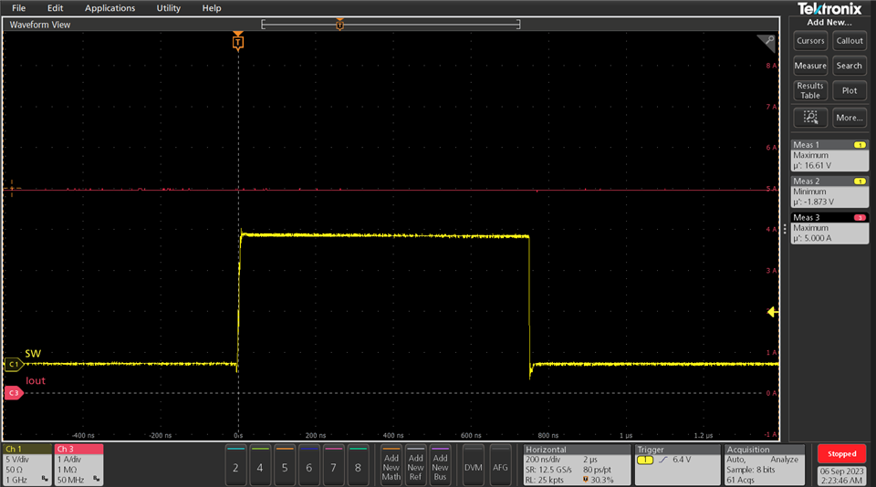
Figure 4. SW-GND_Zoom in

  • Hello,

    I will need some time to review the schematic. If the application is for 12Vin but the voltage on the SW/GND on time is above 15V DC, then I suspect there is some issue in the schematic and probing.

    Also have you checked out this out on the LM61495RPHEVM, configured for your application and recreate the same issue? I would suggest starting with the EVM and then we can compare the SW on EVM with SW on your board with your test setup.

    Regards,

    Jimmy

  • Hi Jimmy, 

    Sorry to make misunderstanding. I forgot to mention maximum input voltage is 16V, so I used this condition to check phase node voltage.

    I agree test EVM is a good idea, but I would like to check the waveform at first, since another power rail on this board alos has similar behavior.

  • Hello Alex,

    The high frequency component on the SW node is usually a result of the fast edge SW node rising transition. 

    You can further attenuate this ring by one of two things:

    1. Use the R_RBOOT resistor to slow down the rising edge SW slew rate to reduce the ringing
    2. Add a RC snubber circuit to dampen the ring within one cycle, steps to design the RC snubber: (https://e2e.ti.com/blogs_/b/powerhouse/posts/calculate-an-r-c-snubber-in-seven-steps).  

    Regards,

    Jimmy

  • I tried to add snubber and Rboot on this circuit, and adding snubber might provide a minor improvement.

    For the Bboot vaule, I put 100ohm, and the ringing become smaller, but this Rboot value might cause unknow side effect.

    I'd like to check with you. Is this ringing can be acceptable? The ringing is still there even putting Rboot 100ohm.

    Please see the following waveform

    1. Original SW-GND w/ 2.7A

    2. SW-GND w/ 2.7A, Snbber: 470pF & 1ohm

    3. SW-GND w/ 2.7A, Snbber: 470pF & 5ohm, Rboot:2.2ohm

    5. SW-GND w/ 2.7A, Snbber: 470pF & 5ohm, Rboot:100ohm

    Thank you,

    Alex

  • Hello Alex,

    The ringing may still be there but the peaking of the switch node is significantly reduced. 

    The point of reducing this ring is to minimize the conducted emissions (CE) and radiated emissions (RE) to meet the typical standards.

    In addition to the input EMI filter, RBOOT and RC switch snubber will help to minimize EMI results. 

    This device is operational and regulating, whether it is acceptable or not depends the system application's CE and RE result and your design requirement for noise emission. For most customers, the switch node waveform you have is okay.

    Regards

    Jimmy

  • Hi Jimmy,


    Thanks for your clarification for the ringing behavior.

    Also, for the question 1 mentioned above, the voltage of SW-GND is lower than Vin-SW.

    Is this a common case? How’s the reason cause the phenomenon?

  • Hello,

    If you are reading the "Measure1" value from the two curves then Vin-SW is measuring higher because it is capturing the highest voltage reading which looks like the ring. Compared that to the actual SW-GND ring, the Vin-SW measurement shows more peaking. What is the reason why you need to measure Vin-SW? 

    From application point of view, the buck converter looks to be operating properly and SW-GND shows the device switching from voltages Vin (16V) to GND (0V) which makes sense for a buck device. 

    Regards,

    Jimmy  

  • Hi Jimmy,


    Thanks for your reply.

    Capturing Vin-SW waveform is used for check the internal high-side MOSFET behavior. Many clients require test this data for phase node measurement.