


Hi Everyone,
I have downloaded the PLECS simulation model of the LMG3522R030 device and thereby I obtained remarkably low temperature rise of the GaN FET.
For test purpose, I checked the behaviour with a simple Buck configuration (switching frequency 100 kHz), as it can be seen in the attached PLECS model. Thereby, switching 78 [A] at 400 [V] results in a junction temperature rise of only around 6 [°C] (for the high-side GaN FET). On the other hand, the calculation of conduction and switching losses seem to be coherent.
Hence, I checked the thermal description, whereas the following model parameters are present in the LMG352xR030_V1.xml file (attached as well):
FET:
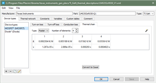
sum(Ri_fet) = 0.056618 [K/W]
DIODE:
sum(Ri_diode) = 0.158798 [K/W]
One can see that the sum of the thermal resistors is not equal to the steady state thermal resistance of 0.28 [K/W] indicated in the datasheet.
Finally, my questions are:
- May there be a bug in the thermal description LMG352xR030_V1.xml?
- Additionally, I have seen that in the FET's Turn-Off Losses Look-Up Table, the turn-off energy Eoff = f(v,i,T) is only specified for fixed v = 400 [V] and T = -40 [°C]. Is it planned to provide more information in there?
Already thanks for the support and kind regards,
Nicolas
