Hello,
My customer is concerned about how to design core power.
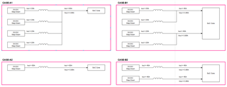
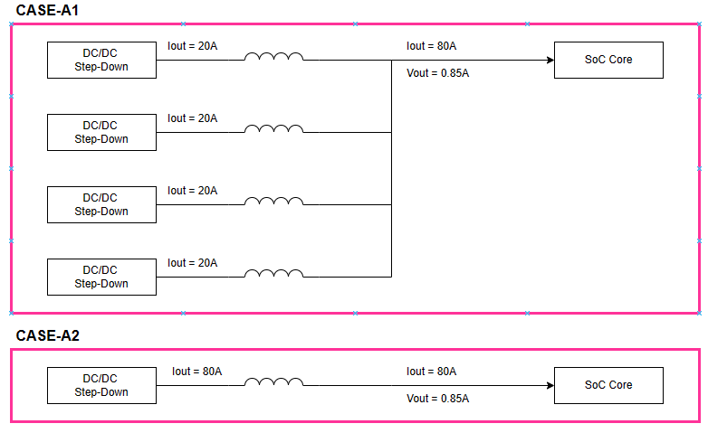
1. What is the difference in efficiency between Case-A1 and Case-A2?
If the conditions are the same, which case has the advantage in terms of efficiency, and is there any data comparing it in approximate numbers?
2. Is there a difference in reliability between Case-A1 and Case-A2?
3. Between Case-A1 and Case-A2, which case is better in terms of heat generation? If you have any example materials, please share them.
4. In case of Case-A1, are there any specification limit issues in design, operation, and use when using the Adaptive / dynamic voltage scaling function?
5. How will it work if one or more of the four parts in Case-A1 is defective?
6. Are there many cases where Case-A1 has been used and proven in the field?
Thank you.
JH