This thread has been locked.

If you have a related question, please click the "Ask a related question" button in the top right corner. The newly created question will be automatically linked to this question.

UCC28C56H: power transfer function

Part Number: UCC28C56H
Other Parts Discussed in Thread: TLV431,

Hi team,

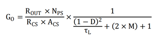
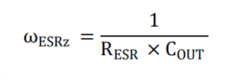
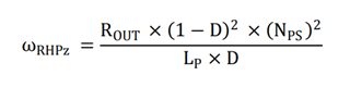
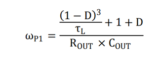
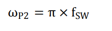
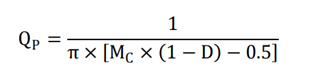
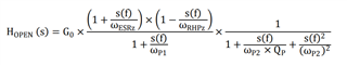
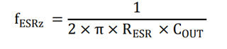
1. What is the specific polynomial of s(f) in this equation in the datasheet?

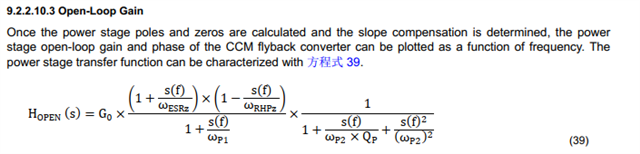
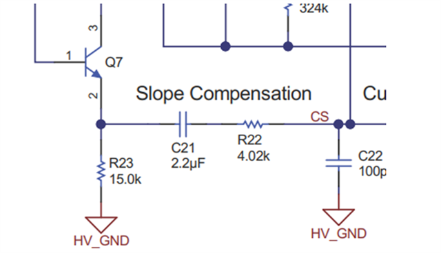
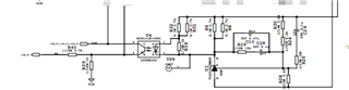
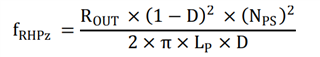
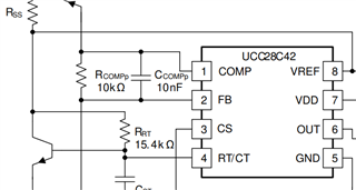
2.Can you provide me with the Complete power transfer function based on the circuit of fig 9-3 in the datasheet?

Thanks

Lillian

  • Hi Lillian,

    s(f) means that 's' depends on frequency. s=j*w. You can consider it as just 's'.

    Thank you.

  • Hi Manuel,

    Thanks for your reply.

    Could you help for the second question, provide with the Complete power transfer function based on the circuit of fig 9-3 in the datasheet?

    Thanks

    Lillian

  • Hi Lillian,

    I will take care of this thread and I will be back to you soon today.

  • Hi Manuel,

    Thanks, look forward your reply.

    Another question is compared with the typical application in the datasheet, the slope compensation loop in the schematic diagram of UCC28C56EVM adds the resistor R23. What is the function of this resistor? How will it affect the open-loop transfer function of the system?

    Thanks

    Lillian

  • Hi Lillian,
     

    Rout: Resistive load of the Flyback converter.

    Nps: Primary to secondary turns ratio of transformer

    Rcs: Current sense resistor.

    Acs: Current sense gain of the IC. See Electrical Characteristics of datasheet.

    D: Max duty cycle, check equation 20 of datasheet.

    t_L: check equation 21 of datasheet.

    M: check equation 21 of datasheet.

    Resr: Equivalent series resistance of output capacitor.

    Cout: Output capacitance.

    Lp: Magnetizing inductance of transformer seen from the primary side.

    Consider max duty cycle.

    Here, the ideal value for Qp is Qp=1, depending on the design of the slope compensation. Please, read section 9.2.2.10.2 for more details.

    Finally, you can replace all of these values in your open loop gain transfer function:

  • Hi Lillian, R23 is a pull-down resistor that assures the turning off of Q7 when it is not conducting.

    Thank you.

  • Hi Manuel,

    Thanks for your reply!

    Another question is during debugging, I found that when the power input voltage is adjusted, the control frequency of the out output will change and never reach the set value. RTCT is externally connected to 15k and 1000p. According to datasheetP16, the switching frequency should be around 110kHz. When my power input is 200V, the oscilloscope's switching frequency is about 30kHz; when the input increases to 600V, the oscilloscope's switching frequency is about 60kHz. The above situation occurs when the output is lightly loaded. When the output is heavily loaded, the switching signal will be missing for several cycles, causing the high-frequency transformer to whistle. Do you have any solutions to the above two problems or explain why they occur?

    Thanks

    Lillian

  • Hi Lilian.

    I am taking care of this thread and I will be back to you soon today.

  • Hi Lilian,

    Please share your schematic, so I can provide the support you need. Also, if possible, share any waveforms in the oscilloscope that show the issues you are mentioning.

    Thank you.

  • Hi Maunel,

    Pls check the schematic here.

    Test waveform shows below:When high voltage is input, the frequency is lower than expected and the cycle is not stable; when the power is turned off, the switching frequency and duty cycle are as expected (scope251)

    And if possible,could you share your mail address? I could contact you by mail.

    Thanks

    Lillian

  • Hi Lilian,

    1. First, please confirm: The waveforms that you showed are taken from OUT-GND from the IC? Just as a tip: I recommend using Tip and Barrel connectors when measuring your output signals with the scope probe (see below). This connector allows to measure with minimum parasitic inductance and improve the accuracy of your measurements. Under what conditions are each of the waveforms taken? Load? Low, high voltage?

    2. About the first two waveforms: 

    -At light load, Flyback converters run at minimum on time, that is why you are seeing minimum pulses at the output driving signals.

    -These driving signals have a switching frequency of few KHz (<5KHz) and that does not match your RT/CT values. Please, place scope probes on RTCT, COM and Isense pins when taking these driving signals. These signals will help to debug and find an answer for the mismatch in the switching frequency.

    3. About the third waveform:

    - OUT signal is turning OFF because Vdd is reaching UVLO_OFF=15.5V. It probably means the auxiliary winding of your transformer is not providing enough current to Vcc to run the IC. It might happen at light load.

    -These pulses/driving signals are at much higher frequency. Please confirm the load conditions here.

    Thank you.

  • Hi Maunel,

    1.We take the waveforms from OUT-GND but the same with above and it seems all works well with RTCT, COM and Isense pins.

    2. We also find a strange consition: 

    We tested on the EVM board again. If we use an ordinary 350V oscilloscope probe, there will be a slight whistling sound. If we use a high-voltage differential isolation probe, there will be obvious whistling sound on the board. Could you reoccur this in EVM?

    The U4 position is a TLV431. We found that if we clamp the probe at the TP8 position for testing, there will be no howling, but the frequency will be slightly lower than the set value. However, if we remove the probe, there will be howling and the frequency will be unstable.

    In addition, we replaced the LMCC capacitor at C10 with a tantalum capacitor. The original Vout=12.9V will become 11.9V. It seems that the compensation has been changed. Please help confirm the cause of this phenomenon. Finally, can you provide the design instructions for the SSR mode?

    You can send it to my mail:lillian-liu7@ti.com

    Thanks 

    Lillian

  • Hi Lilian,

    -For OUT-GND measurements I recommend using a single probe with Tip and Barrel connector (see below). You can connect the probe directly to the OUT-GND pins and get more accuracy and avoid any parasitic components.

    -Are you using UCC28C56EVM? I do not see any U4 (TLV431) or TP8 in the schematic (see below). Also, the output voltage Vout for this EVM is 15.2 for 125V<Vin<1000V. Please, confirm what EVM are you evaluating.

    -I do not understand the last part mentioning SSR mode design instructions? Would you please explain SSR?

    Thank you.

  • Hi Manual,

    Thanks.

    I am sure that we all use the Tip and Barrel connector to test.

    For this part below , we did on the EVM.

    "We tested on the EVM board again. If we use an ordinary 350V oscilloscope probe, there will be a slight whistling sound. If we use a high-voltage differential isolation probe, there will be obvious whistling sound on the board. Could you reoccur this in EVM?"

    Below we did on customer's board.

    The U4 position is a TLV431. We found that if we clamp the probe at the TP8 position for testing, there will be no howling, but the frequency will be slightly lower than the set value. However, if we remove the probe, there will be howling and the frequency will be unstable.

    In addition, we replaced the LMCC capacitor at C10 with a tantalum capacitor. The original Vout=12.9V will become 11.9V. It seems that the compensation has been changed. Please help confirm the cause of this phenomenon.

    This question is urgent now, could you help check first?

    Thanks

    Lillian

  • Hi Lillian:

    1. When testing the OUT-GND driving signal, you can use an ordinary oscilloscope probe, no need to use a differential probe. The slight whistling sound would occur when probing signal waveforms as they are more perceptible to noise when there is coupling coming from the probe.

    2. In the UCC28C56EVM-066, which is the EVM for UCC28C56H, there is no U4-TLV431. The only TLV431 that I find is in your schematic and it has a designator of U1 (see below). Be careful when probing in TP8. The coupling might affect the forward current of the opto-coupler diode and then change the feedback current to the IC and then change your compensation loop and the frequency that the IC operates. Please, verify the correct connection of U1-TLV431 and be gentle when probing there. This device affects directly your control loop.

    3. Tantalum capacitors are electrolytic capacitors, and they have lower resonance frequency than ceramic capacitors. This change might affect the low impedance of the cap at high frequencies and then the compensation transfer function. I recommend using a ceramic cap for C10 in your schematic.

    Thank you.

  • Hi Lilian,

    1. Compensator zero design: C28 and R29 have good values considering a BW=fsw/10. However, C10 should be very low compared with C28 to add a high frequency pole to compensate the gain of the compensator zero. I recommend using C10=C28/10=10nF. 

    3. Compensator pole design: The placement of this pole depends on fesrz/frhpz, whichever is the lowest (see below equations). Place compensator pole fcompp equal to the lowest of those two value. Please, keep in mind that you need Rcomp and Ccomp connected in parallel (see below). In your schematic, it doesn't look like that. You can start chosing Rcomp=10kohm and then calculate Compp with the equation below.

    For more details, please refer to Section 9.2.2.10 of Datasheet.

    Thank you.