This thread has been locked.

If you have a related question, please click the "Ask a related question" button in the top right corner. The newly created question will be automatically linked to this question.

UC3825A: why use uc3825A ?

Part Number: UC3825A
Other Parts Discussed in Thread: UC3825,

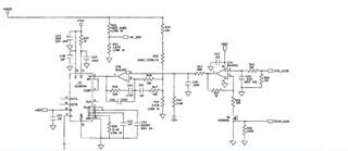
This is an applied circuit diagram, with pins 11 and 14 connected to the gate driver and full bridge MOS to obtain the final voltage output in the upper left corner. And this voltage output is not regulated, it changes at any time. Since there is no need for voltage stabilization, why not directly add PWM signals to pins 11 and 14? What is the significance of the voltage output of this application circuit being fed back, combined with external control signals, and then flowing into UC3825? What role does UC3825 play?

这是一个正在应用的电路图,其11、14脚去连接栅极驱动器和全桥MOS,得出左上角最终的电压输出。而这个电压输出不是稳压,是随时变动的。既然无需稳压,那为何不直接在11、14脚上加PWM信号?这个应用电路的电压输出最终再反馈回来,和外部控制信号一起作用后再流入UC3825,有什么意义呢?UC3825起到什么作用呢?

  • Tom Tom,

    Since you've only showed a partial schematic, I can't say for sure but there is a feedback signal being used to control the pulse width OUTA/B. The "SYS_ECON" signal is being used as feedback to the UC3825A. The DC gain and control loop compensation are set up externally using the two stages of MAX492A (U7A/B). The UC3825A, internal error amp is only used as a buffer, The UC3825A is used as a voltage mode PWM control to vary the OUTA/B pulse width according to the SYS_ECON and +HVDC. +HVDC is not regulated because there is no reference used in the feedback. +HVDC is divided down and applied as a voltage reference to U7B-6 but the system has a varying reference (+HVDC) and assumedly a varying control signal (SYS_ECON).

    Regards,

    Steve

  • 一般传统的DCDC控制芯片内部,在外围环路补偿电路基础上,以反馈电压和内部参考电压做误差放大,去和某三角波做切割得出脉宽。
    从你的意思里,此电路图外围环路补偿电路,以及反馈电压和内部参考电压误差放大,这两块都去掉,直接用SYS_ECON反馈电压和外部参考电压误差放大。但UC3825内部框图还有个3脚和7脚1.5V参考电压的比较。难道有两个参考电压:一个是固定的1.5V,一个是变动的?
    另外,那个ECON_GAIN起调节直流增益作用吗?

    In general, traditional DCDC control chips use feedback voltage and internal reference voltage to amplify errors based on peripheral loop compensation circuits, and cut with a certain triangular wave to obtain pulse width.

    From what you mean, this circuit diagram includes the peripheral loop compensation circuit, as well as the feedback voltage and internal reference voltage error amplification. Remove both blocks and use directly the error Amplify between the SYS_ECON of feedback voltage and the external reference voltage. But there is also a comparison of the 1.5V reference voltage between pin 3 and pin 7 in the internal block diagram of UC3825. Are there two reference voltages: one is fixed at 1.5V and the other is variable?

    Also, that ECON_ Does GAIN play a role in regulating DC gain?

  • Also,Does that ECON_GAIN play a role in regulating DC gain?

  • Also, both variables are variable variables, How do you control SYS_ECON and the reference voltage after output voltage reduced?  Which of the two variables does the control result depend on?

  • You have to consider the dynamic range of both variables to have any understanding how the PWM might be responding. 

    steve