This thread has been locked.

If you have a related question, please click the "Ask a related question" button in the top right corner. The newly created question will be automatically linked to this question.

UCD90160A: [Consultation] UCD90160ARGCR Schematic review request

Part Number: UCD90160A

Hi TI service team,

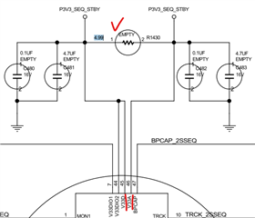
Could you help to review attached SCH file for "UCD90160ARGCR" HW design check ?

Please help to regard all parts as stuffed components in design.

Thanks.

TI_UCD90160A_SCH_CHECK_V1.0_20231106 (with WM).pdf

  • By the way, here are some details of my circuit design:

    1. VMON is about 1.6V divided voltage into UCD90160A for voltage sensing

    2. GPIO for ENABLING external power IC has pull-down to GND with 100K ohm

    3. Brownout circuit has 517uF CAP + 2200uF bulk CAP to sustain VDD (2.9V --> 2.6V)

    4. GPI like below signals have over 2.2V voltage level into UCD90160A

    - PGD_P50V_1_PVRM123_CS (2.2V)

    - PGD_P50V_2_PVRM456_CS (2.2V)

    - PGD_P50V_1_PVRM123_SEQ_R (2.47V)

    - PGD_P50V_1_PVRM123_SEQ_R (2.47V)

  • Hi

    Please follow this sch design guideline.

    1. not see voltage divider resistors

    2. the TRST shall have 10K pull down and it is missing

    3. FPWM pins are by default output as low. do not use them for any power supply with ACTIVE low enable.

    Regards

    Yihe

  • Hi Yihe,

    Can you also help to check HW design of decoupling capacitors at VDD (V33DIO1 / V33DIO2 / V33D / V33A / BPCAP) related pins ?

    Please check my feedback for your questions as below:

    1.Voltage devider resistors:

    12V:

    3V3:

    50V:

    2.TRST has pull-down resistor with 10K ohm to GND:

    3.FPWM pins for power IC EN are all ACTIVE "high" enable function

    Best Regards,

    Paul Lei

  • Hi

    The decoupling caps are listed in the https://www.ti.com/lit/pdf/slvub50 

    Please follow.

    Regards

    Yihe

  • Hi Yihe,

    I have checked the "SLVUB50C" document for my HW SCH/layout design in previous, but I have two questions want to confirm with you as below items at last.

    Thanks.

    #1 If I have applied brownout circuit in my HW design, could I connect UCD90160A power supply with after Schottky diode, not directly to 3V3 power supply like file described?

    SLVUB50C:

    Brownout circuit in datasheet:

    #2 Is it correct with my HW schematic design in comparison with SLVUB50C described (4.99ohm connect with V33D and V33A)?

    Please regard my HW schematic screenshot as stuffed components, not empty parts.

    SLVUB50C:

    My HW design:

  • Hi

    1.if you have the brownout, the VCC shall be after the diode.

    2. Yes, 4.99ohrm between V33A and V33D is needed.

    Regards

    Yihe