Hi,
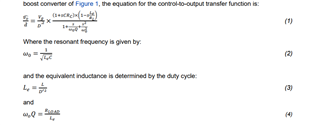
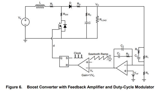
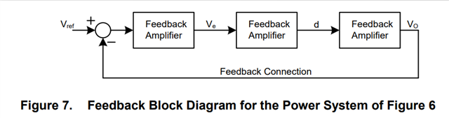
I am designing a voltage mode controlled boost converter for which I have choosen type 3 compensation. Also I am aware of TI' s power stage designer(which dosent have option for Voltage mode control of boost).I want to know how to place poles and zeros for type 3 compensation, so I came across SLVA633 application note which is good but It will be helpful if there is closed loop control design example for boost converter or a calculator spreead sheet to validate the design results. Also in SLVA633 I am confused about D' is it obvious duty cycle or (1-D) also what is d^ ?