부품 번호: LMQ61460
This is a circuit with an output voltage of 8.7V for a 12V input.
The output voltage is not output properly.
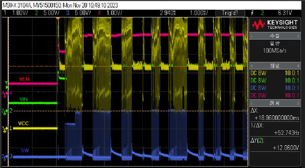
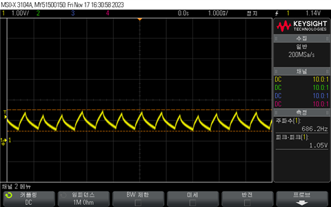
The picture below shows the waveform of the output.
It does not output up to 8.7V. What could be the problem?
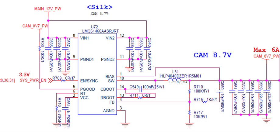
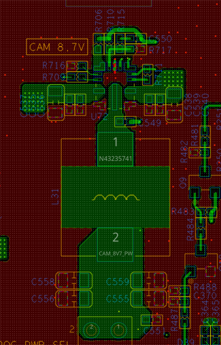
부품 번호: LMQ61460
This is a circuit with an output voltage of 8.7V for a 12V input.
The output voltage is not output properly.
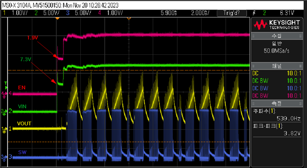
The picture below shows the waveform of the output.
It does not output up to 8.7V. What could be the problem?