This thread has been locked.

If you have a related question, please click the "Ask a related question" button in the top right corner. The newly created question will be automatically linked to this question.

LM5106: Ringing/oscillation issue

Part Number: LM5106

Hello,

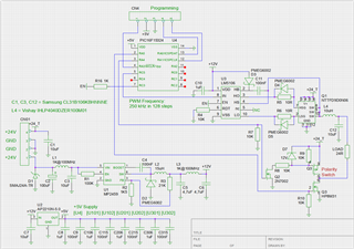
I'm working on a PWM controlled voltage source using an LM5106 half-bridge MOSFET driver, with a PIC16F15324 supplying the PWM signal. This PWM signal has a frequency of 250 kHz, and a duty cycle step size of 1/128 = 31.25 ns (~ 0.78%).

The problem is that I'm having a serious ringing/oscillation issue that so far, I haven't been able to solve. One curious feature of the ringing is that it only occurs at very low or very high duty-cycles, but not in between.

As the ringing occurs at approximately 100 MHz, I must get rid of it if I want this product to comply with basic EMC regulations. However, nothing I tried so far has helped.

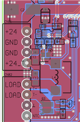
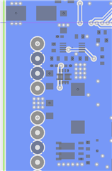
For reference, here's the schematic:

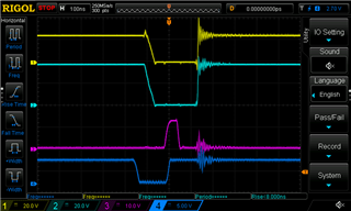
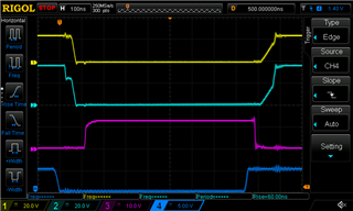
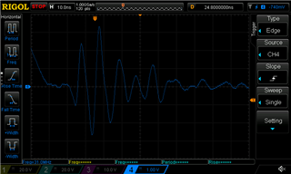
And here is what I see on my oscilloscope at a low duty-cycle (2.3%):

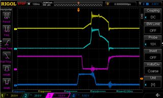
Trace number legend:

  1. Yellow: half-bridge output (HS)
  2. Cyan: high MOSFET drive signal (HO)
  3. Magenta: low MOSFET drive signal (LO)
  4. Blue: PWM input (IN)

The ringing is clearly associated with the high-side MOSFET switching on and off.

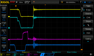
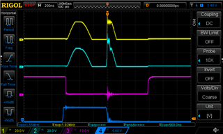
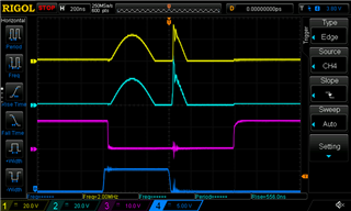
Things are even worse at maximum duty cycle (97%), probably because of the higher overall output current:

A thing to note here is that the switching edges become much steeper at these low and high duty cycles - and these faster rise times are no doubt also what cause the ringing in the first place.

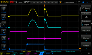
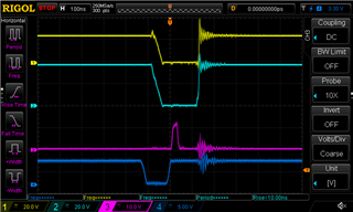
The following image shows what the signals look like over most of the duty cycle range, and what I would expect:

Clean sloping edges, without ringing.

About the MOSFET device (NTTFD9D0N06HLTWG): this is an integrated half H-bridge with two nearly identical MOSFETs. These MOSFETs have an input capacitance of approximately 1 nF and an output capacitance of about 500 pF, which should be just fine.

So the question is of course where the ringing comes from, and how I can eliminate it. Given the curious behaviour of the drive signals, I think I'm overlooking something about the LM5106, but despite spending quite a bit of time on the problem, I haven't been able to find the cause.

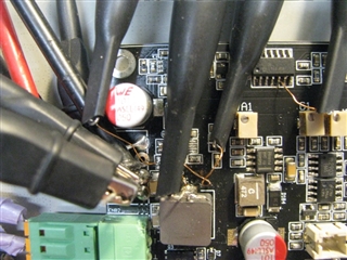
If it helps, I can also submit an image of the PCB layout, in case there's a problem with the geometry. Generally speaking, I put everything as close together as possible, with an almost uninterrupted ground plane on the bottom layer and a lot of stitching (vias) from GND connections on the top layer to this bottom layer.

Any help is appreciated.

Regards,

Richard

  • Hi Richard, 

    Our expert on this device is currently out of office for the Thanksgiving holiday. Please expect a response early next week. Thank you! 

    Vivian

  • Thanks Vivian.

    Hi Richard,

    Thanks for reaching out to us.

    Did you try removing D4 and D5? If fall time ends up being too slow then you may try reducing the gate resistor from 10 Ohm to 2.2 Ohm or whatever suits/meets the design requirment.

    Please let us know and we can take a look into it in more details.

    Thanks and regards,

    Ritesh 

  • Hello Ritesh,

    Thank you for your quick reply! I tried shorting R5 and R6, of course effectively removing D4 and D5 as well.

    In addition, I mounted small HF bypass capacitors (100nF || 1nF) parallel to the large 10uF capacitors, in particular C1 and C12 (which have a self-resonant frequency in the 4-5MHz range).

    Unfortunately, this did not make any difference:

    The main question is why the positive-going edge is so much steeper at these high (or low) duty cycles than somewhere in the middle range. It would appear that these shorter low-going phases in the 100-200 ns range somehow cause resonance, causing the positive-going edge to rise much faster than would otherwise be the case (see the last image of my first post).

    Just for the sake of completeness, here's an image of the relevant part of the PCB:

    Here's the same area, now just the bottom layer:

    It's a solid ground plane with cut-out traces for the high-side MOSFET gate (left) and the HS signal.

    Long ago, I experienced similar problems due to cut-outs in a GND plane, effectively causing resonant loops - but those were much larger, and could be fixed easily by making the cut-outs smaller. These traces are so short that the encompassing GND loop should not produce resonance in the 100MHz range.

    But just to make sure, I laid two small GND bridges across both of these traces in the bottom layer. As expected, it did not make any difference at all.

  • Hi Richard,

    By shorting R5/R6 you did effectively removed the diode effect, but it would not help reduce the ringing because now you increased your turn-ON speed as well.

    Thus, I would again recommend that if you dont need fast rise/fall time of the power switch then remove those gate diodes, keep the gate resistor. This will slow down the gate and should reduce the ringing.

    Apart from switching speed, the gate drive loop inductance and power switch parasitic elements are the key elements contributing to the high frequency ringing. By reducing the gate drive loop we can reduce the ringing but it is iterative process and many a times not feasible (depending on the stage of the project).

    My colleague, William, may also add some of his comments here.

    Regards,

    Ritesh

  • Hello Ritesh

    Shouldn't the diodes only affect the switching off of the MOSFETs? The problem occurs when the high-side MOSFET is switched on, not off - and only the high-side MOSFET, not the low-side one.

    Also, I can't possibly make the gate drive loop any shorter - it is as short as it can be. Laying a wire from the MOSFET switch output directly to C11 (bypassing the slightly longer loop to the right) did not make any difference.

    Anyway, just to make sure, I restored the 10 Ohm gate resistors and removed the diodes, and as I already expected, this did not change anything. This is what the signal looks like at 95% duty cycle:

    And as before, the problem goes away when the duty cycle is moved away from the highest (or lowest) values. This is what 73% duty cycle looks like, with the ringing almost gone and a rising edge that isn't as steep:

    It almost looks like that at small (either high or low) duty cycles, so pulses <200 ns or >3.8 us, the LM5106 has a much increased gate drive capability as compared to mid-range duty cycles. So maybe the bootstrap capacitor C11 has something to do with it?

    However, first I tried increasing the gate resistors to 47 Ohm to see what that would do. Unfortunately, this destroyed the high-side MOSFET almost instantly, even with 500 mA current limit on the 24V supply.

    After replacing the dual MOSFET, the LM5106 and restoring the gate resistors to 10 Ohm (still without the diodes), I increased the dead time resistor R4 to 100K, just to be on the safe side - this should provide some 550 ns of dead time to protect the MOSFETs during experiments; for good measure, I also increased the bootstrap capacitor C11 from 100nF to 1uF, so that gate drive current should not be a problem either.

    The result was quite unexpected:

    Not only does switching on the high-side MOSFET still cause the same ringing as before, and with the same weird edge behaviour as before, there is now also a very strange half-sine-like waveform preceding the actual switching on.

    I have no idea what to make of this, except that it must have something to do with the LM5106 supply or boost circuit. And oh, increasing the duty cycle from here eventually destroys the high-side MOSFET again, probably because of excessive power dissipation due to being half switched on for a lot of the time. Something clearly is very wrong, but I can't figure out what it is.

    So I'm pretty much at a loss here. I think I tried everything that I could, but all my changes so far either did nothing or even blew things up. The strange thing is that I used the LM5106 before on several occasions in almost the same configuration, except that I used single MOSFETs then, with a larger input capacitance, a larger inductor and a rather different PCB layout (one of which caused ringing too, but that was easily fixed).

    Does anyone have any ideas what may cause this strange behaviour?

  • Hey Richard,

    I am a colleague of Ritesh's and wanted to add some insight here.

    How are you taking these measurements to see the ringing?
    In situations where we see excessive ringing, we advise using a tip and barrel probe at the pins of the driver as well as setting the oscilloscope to AC coupling and full bandwidth mode. This allows you to capture the ringing accurately to ensure what is happening in the circuit is what you are seeing.

    Are you able to add a bootstrap resistor and see if this improves this ringing and overshoot? One possibility is that you are seeing overcharging of the bootstrap capacitor in the low duty cycle scenario. That doesn't answer why this occurs during the high duty cycle scenario too but it could provide insight on if the bootstrap capacitor is overcharged.

    Let me know what your findings from my questions are and if you have any further questions.

    Thank you,

    William Moore

  • Hi William,

    Thank you for joining this rather tricky puzzle session!

    I am using the standard oscilloscope hook probes with ground clips, with small bits of shellac-insulated transformer wire soldered to the actual measuring points. All the ground clips are clamped onto one thick bit of GND wire soldered to one of the GND connections shown in the PCB image above.

    This is what it looks like from above:

    Yes, I know that a tip and barrel probe method gives much cleaner results, but since I have so far failed to realize the electronics engineer's dream of growing several extra sets of hands, I can only measure one signal at a time that way. And even then, manipulating the controller input and the oscilloscope takes quite a bit of juggling.

    Anyway, I changed C11 (C-bootstrap) back to 100nF again, and put a smallish bootstrap resistor in series. At 10 Ohm, nothing changed, with the oscilloscope picture still identical to the last one. With R-bootstrap=100 Ohms, the ringing diminished somewhat, but everything else remained the same, including the strange hump during what should be the high-side MOSFET's dead time:

    Now I could of course reset the dead time to some more sensible value by decreasing R4 to 10K again - this would no doubt eliminate the hump, but then I'm back to square 1. Then again, at least things should no longer blow up then, and I could also measure the ringing frequency more precisely then - although I don't know if that is very informative.

    The main question that I think I need to answer is what causes the edges of the high-side drive to become much steeper at very low and high duty cycles, leading to oscillation, while returning to a far more gentle slope in between. And this is probably also related to this mysterious hump - which looks a bit like part of a 2-3 MHz signal, and that is roughly the same as the resonance frequency of the 10 uH inductor and the combined MOSFET output capacitance (380 pF).

    So maybe these short pulses (both at high and low duty cycles) cause the MOSFET switch + inductor to resonate at a few MHz, driving current back through the top MOSFET source capacitance to the gate, forcing a steep turning-on? Then again, I never saw anything like this happen before, not even in my more Frankensteinish creations, with neighbours complaining about TV interference ...

  • Another observation: I measured the RF ringing (see below), and introduced extra capacitance from the MOSFET switch output (HS) to GND to see if that made a difference.

    This is the HF ringing without the extra capacitance, as measured on the IN(!) signal, so the bottom trace in the above oscilloscope images:

    And this is the same IN signal, now with a 470pF ceramic capacitor from HS to GND:

    The amplitude is somewhat lower, but the frequency has essentially not changed. Which means that the HF ringing is not dependent on the capacitance at this point, but seems to come from the LM5106.

    However, the 'hump' does appear to be notably wider, so this lower-frequency resonance does stem from the LC combination at the MOSFET switch output:

    The puzzling thing is that literally nothing I tried so far made any difference to the core problem. I tried increasing (and diversifying) capacitors on the +24V and +12V supply lines, introduced extra GND bridges across the two bottom layer traces, and tried different gate resistors, a bootstrap resistor and several small capacitors at different places just to see what would happen. During all this, the RF ringing stays a solid 100 MHz signal, only slightly suppressed by capacitors, but not changed in any other way, let alone eliminated.

    My experience tells me that the most likely cause is still the PCB geometry, but I have no idea how that can be improved - I kept everything as close together as possible, with a closed GND plane at the bottom except for two short traces.

  • Hey Richard,

    It looks like you could be experiencing a "quiet" switching condition where the power train is soft switching or mostly soft switching. This occurs where the drain of the MOSFET transitions or mostly transitions from low to high during the dead time.

    For the ringing on the waveforms, it looks like hard switching is occurring when you turn off the low side FET. This occurs when the body diode starts conducting (switch node stays low) and when you turn on the high side, the switch node dV/dt is a lot higher due to forcing the body diode of the low side FET off.

    For softening this hard switching, you can increase turn on resistance of the high side FET or utilize a FET with faster body diode recovery.

    Let me know what your findings on this are and if you have any further questions.

    Thank you,

    William Moore

  • Hello William,

    First of all, and once again, my thanks for your continuing support and input. I really appreciate it, even though so far, it hasn't brought me any closer to a solution.

    I don't quite understand how this 'quiet switching' or 'soft switching' works; I'll see if I can find more information on that.

    For the ringing on the waveforms, it looks like hard switching is occurring when you turn off the low side FET.

    I'm afraid I don't share your analysis here - quite the contrary: as far as I can see, waveforms do not show any relationship between switching the low-side MOSFET and ringing in the high-side MOSFET. Here are two traces that I showed earlier, one with a short dead time and a high duty cycle, and the other one with a very long dead time and a low duty cycle:

    Trace #3 (magenta) is the low-side MOSFET gate signal. In either case, switching this gate on or off hardly causes any visible ripple in the other signals. (The slight ring in trace #4 upon switching off the low-side MOSFET is an HF artefact picked up through the ground loop, and disappears when using the tip-and-barrel method.) However, when the high-side MOSFET turns on, this causes a strong ringing on all lines.

    Also, when switching the low-side MOSFET causes the ringing, then shouldn't this happen all the time, regardless of the duty cycle? Because there are no problems at all when the duty cycle is somewhere between 25% and 75%, like here:

    It is quite strange to see the high-side MOSFET drive signal changing from very steep (and ringing) to more gently sloping with increasing duty cycle, and back to very steep again at the end - I could try shooting a video of it, if that would give you people a clearer picture of what I see happening.

    About the body diode: reverse recovery time is given in the datasheet as 29 ns (starting from 19 A, with dI/dt = 100A/us), which is faster than in most other MOSFETs that I used without any problems. So I don't think that a slow body diode is causing this. But I'll first dive into the mentioned phenomenon of quiet/soft switching, to see how that works. Do you happen to have any links to development notes about this?

    Anyway, trying another MOSFET or increasing its on-resistance would require creating and ordering a new PCB in order to accommodate the new device, and that would take at least a couple of weeks, or more likely even a month, what with the holidays coming up.

    BTW, I could duplicate the circuit and physically send it to you for testing, if this is something that you do - I still have a couple of boards in stock. Yes, this is something that I really should figure out for myself, but I must admit that this problem has me stumped.

    But thank you again, regards,

    Richard

  • Hey Richard,

    What you are seeing is hard switching when the high side turns on, this is due to the inductor discharging through the low-side body diode. When the high-side turns on, it has to force the low-side body diode off and during that time that it is forcing that body diode off, you get this high dV/dt scenario with the high side turning on and the ringing.

    To reduce the ringing on the high side, you can do a couple things:

    Slow down the turn on of the high side FET by having a higher turn on gate resistance.

    Use a low side FET with a faster recovery body diode.

    Add a snubber on the switch node. For that you can reference this thread "Power Tips: Calculate an R-C snubber in seven steps".

    Let me know if you have any further questions.

    Thank you,

    William Moore

  • Hello William,

    Thank you for your latest comments; they finally made me get a grip on things. Here's the current set-up

    • I now use a 47 Ohm gate resistor R5 to significantly slow down the switching-on of the high-side MOSFET;
    • I put a 10 Ohm resistor in series with the gate diode D4 to also slow down the switching-off - but not so slow that shoot-through can occur, or an increased dead-time becomes necessary;
    • I calculated a snubber network following John Betten's article - I had experimented with snubbers before, but those were based on commonly used values and experience rather than proper calculations. It turns out that a Csnub of 330 pF in series with a Rsnub of 12 Ohms gives quite good damping already.

    With these measures, I substantially reduced the range where ringing occurs to only the lowest duty-cycle values (up to 1.5%), which I can simply skip in my code. And I think I can still improve on the actual values; I'll do some more experimenting with the gate resistors, and I'll also measure the power loss in the snubber resistor, to determine the maximum practical value for the snubber capacitor.

    The only thing I can't do much about is the MOSFET device, as this one of the very few combining this small footprint with the desired electrical characteristics (Vds-max > 40V, Id-max > 5A). Also, I'm not completely clear about the mechanism that causes steeper switching behaviour at shorter input pulses, and this soft-switching thing during extended dead-time experiments. But I'll try and find more about this on my own.

    So thanks again for your help and insight, it has improved my understanding quite a bit!

    Regards,

    Richard