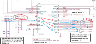
The HD3SS3220 evaluation board schematic shows
RX2P/RX2N and CRX1P/CRX1N are connected to the Type-C side of the TX2p/TX2n and TX1p/TX1p pins, and the receive signal appears to be connected to the transmit port.
However, the datasheet shows a configuration diagram with TX2P/TX2N and TX1P/TX1N connected to the TX2p/TX2n and TX1p/TX1p pins, which is correct?
Is either one OK?

-
Ask a related question
What is a related question?A related question is a question created from another question. When the related question is created, it will be automatically linked to the original question.