This thread has been locked.

If you have a related question, please click the "Ask a related question" button in the top right corner. The newly created question will be automatically linked to this question.

LM5148-Q1: Gate Driver

Part Number: LM5148-Q1
Other Parts Discussed in Thread: LM5148, LM5145, CSD19503KCS,

Hi Team,

This is regarding the buck converter

Input Voltage: 40V-60V

Output Voltage: 13.8V

Output Current: 10A (max)

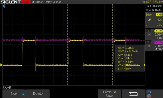
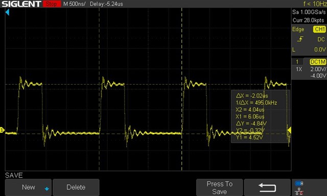
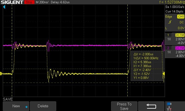
Switching Frequency:500kHz

Gate Voltage: 4.8V (when measured)

I am facing and issue in designing a synchronous buck converter with Gate resistor calculation.

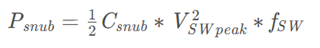
  • Theoretically I am getting the max loss of 7-8W but in practical I am facing 10-20W losses at 50V.
  • Thermal issue: at 75% of load (7.5A-7.8A) upon 2 hour continuous load test the MOSFET is getting heated upto 150 Degrees
  • Can this thermal issue be resolved by increasing the Gate voltage from 4.8V to 10-13V?
  • If above case is possible how can we increase the Gate Voltage from 4.8V to 10-13V? Also specify the HO and LO maximum Voltage rating (Driver Voltage).
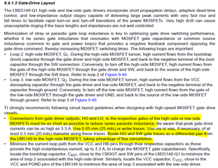
  • What are the HO and LO driver resistance values for the proper Gate resistor Calculation so that Losses and the efficiency are at balance (Not like in the point 1)

Please find the attached Screenshot of the Schematic:

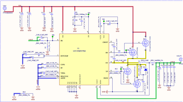
The Resistors R6 & R12 are the Gate resistors replaced by 4.3 Ohm instead of 0 Ohm.

Please provide some clarity on the above questions and also suggest the changes.

Thanks & Regards

Mahankali Nikhilindu Kasyap

  • Hi Mahankali,

    How do you calculate the power loss of mosfet? By calculation tools? From performance, I think the Q1 and Q4 are suitable. In addition, I think you can also refer to the mosfet selection on our LM5149EVM board. https://www.ti.com/lit/pdf/snvu820 

    The driving voltage of LM5148 is related to the VCC voltage. However, it is limited by the VCC withstand voltage, so the driving voltage cannot be increased externally. Have you tested the SW waveform? Is the SW waveform stable at present? Because I'm worried that there are some problems with your current compensation network. You can modify the compensation network by referring to the parameters on LM5149EVM. Hope this can help. Thanks.

    Aurora

  • Hi Aurora,

    The Compensation is according to the Datasheet Formula, where the considered crossover Frequency is 15kHz, and I have verified them with TI Power Stage Designer Tool the compensation graph was similar to that of a stable system and also with the Gate resistors in place the Voltage Spike when ever Q1 was switching reduced.

    Can the High-side MOSFET heating be reduced by adding a snubber circuit at High-Side also?

    And the Pin Graph- Do we need to observe it with a differential Probe with respect to GND? Could you suggest how to measure that Graph!!

    Thanks

    Mahankali Nikhilindu Kasyap

  • Hi Mahankali,

    I'm just worried that the loop might be unstable and cause heating issues. Of course, this can be roughly judged by observing whether the SW waveform is stable. If you think there is no problem with the loop, then there is no need to adjust the compensation parameters.

    Adding a snubber circuit can improve. But I think the current problem may still be caused by the improper choice of mosfet that causes the HS mosfet to heat up. So I would suggest you replace Q2 and Q3 with Q1 and Q4 models. Or refer to the mosfet model on our LM5149EVM.

    What do you mean by PIN Graph? In fact, generally only testing the HS mosfet drive voltage or the voltage of Cboot requires a differential probe. Other waveforms can be obtained by measuring GND with an ordinary probe. Thanks.

    Aurora

  • Hi Aurora,

    Please find the attached Images of the SW wave forms with the test condition.

    Input Voltage: 50V

    Output Load Current: 6A

    SW graph and Input

    Input Voltage: 50V

    Output Load current: 9A

    Only SW Graph

    Input Voltage: 50V

    Output Load current: 9A

    Only SW Graph and Input

    Also Could you suggest how to implement a high side Snubber! And How can we reduce the transient and the Ringing at this SW.

    Thank you

    Mahankali NIkhilindu Kasyap

  • Hi Mahankali,

    I'm sorry for the delay in my reply due to the holidays. For your waveform, I think it may be caused by improper layout of the drive lines ( HO, SW, LO). So if you will change your layout, pls refer to our datasheet for more detail. At present, we can only try to add RC snubber to improve this oscillation. You can put C=1nF, R=5ohm first. Then use the equation below to check the power loss to make sure the resistor can handle. Adding snubber between VIN and SW is to reduce the oscillation on the falling edge of SW. Adding snubber between SW and GND is to reduce the oscillation on the rising edge of SW. Hope this can help. Thanks.

    Aurora

  • Hi Aurora,

    Thanks for the feedback but as I have mentioned in the start that I am observing very high losses than the theoretical losses, and upon ,ore testing and keen observation of the Gate pulse graphs the MOSFET rise time and Fall time are not Matching with the Datasheet values. At the 0 OHM of the GATE resistors the MOSFETS were getting Damaged so we I have replaced them with 4.3 OHM at both low side and high side, and tested.

    Please find the below Table at different loads the Frequency, Rise time and Fall time:

    Case 1: Q1 Gate resistor = 4.3Ohm, Q2 Gate Resistor = 4.3Ohm

        Rise time Fall Time
    Load Frequency Q1 Q2 Q1 Q2
    0 487 64 64 60 29
    1.6 479 84 25 37 30
    2 476 82 23 35 29
    3 489 85 21 29 30
    4 488 83 20 28 29
    5 485 86 20 28 29
    6 482 86 18 26 29
    7 478 83 18 27 27
    8 478 82 18 26 26
    9 480 76 21 26 29
    10 478 74 20 27 28

    Case 2: Q1 Gate resistor = 2Ohm, Q2 Gate Resistor = 4.3Ohm

        Rise time Fall Time
    Load Frequency Q1 Q2 Q1 Q2
    0 474 45 14 61 22
    1.6 479 53 71 38 23
    2 490 54 69 33 24
    3 488 59 65 29 26
    4 487 60 65 26 26
    5 472 60 62 24 28
    6 492 62 63 24 25
    7 478 67 60 24 24
    8 481 65 65 24 25
    9 486 65 60 23 19
    10 489 67 59 24 24

    And the actual Rise time and Fall time of the MOSFETs are 2.5nS and 3nS respectively.

    So could you please clarify what is the relation between the Gate resistor and the Rise time, Fall time changes. Because as I understand the Rise time and Fall time effect the Losses very much.

    Thank you

    Mahankali Nikhilindu Kasyap

  • Hi Mahankali,

    Increasing the gate resistance will slow down the mosfet's turn-on and turn-off speeds. This can increase the dead time and avoid mosfets pass-through. Generally, in order to slow down the turn-on time of the mosfet and keep the turn-off time unchanged, a reverse diode is connected in parallel with the gate resistor.  Do your HS and LS mosfets still use two different types of mosfets connected in parallel? Is it possible to refer to our LM5149EVM to replace the mosfet with similar parameters? 

    Please test the mosfet pin for the actual gate voltage. The HO and LO voltages at the LM5145 chip pins meet the requirements of adaptive dead time control.

    Thanks.

    Aurora

  • Hi Aurora,

    I am in the process of procuring the MOSFETs suggested in the Evaluation calculation sheet provided, but for the better understanding of this MOSFET Losses and the thermal issue. So could you provide any documentation or application note relating the Gate resistor, MOSFET rise time and Fall time and the losses. I think there has been similar discussion and issue in "CSD19503KCS: MOSFET rise time and fall time check" thread! and I think there was a solution provided by @Lucian Hriscu regarding the Rise time and Fall time information. So it would be much more helpful with the better understanding of these values for better selection of the MOSFET.

    Thank you,

    Mahankali Nikhilindu Kasyap

  • Hi Mahankali,

    I just have an AN about power loss calculation of buck circuit. I put it in the attachment. Hope this can help. In addition, based on your waveform, I think there may be some problems with your driver wiring. For details, you can refer to section 9.4.1.2 of the datasheet. Thanks.

     Power Loss Calculation With Common Source Inductance Consideration for Synchronous Buck Converters.pdf

    Aurora

  • Hi Aurora,

    I have gone through the Application Notes that you have attached, but I have a few queries regarding the switching losses.

    For calculating the switching losses in the AN they have used the R_driver and R_g, in which I have not found the R_driver in the LM5148-Q1 datasheet. So which value to consider and calculate the losses!

    Thank you,

    Aurora.

  • Hi Mahankali,

    As LM5148 is a buck controller, so there is no R_driver inside it. I think you should use the Rg of mosfet and the R_driver you add (like R6 and R12) for calculation. Thanks.

    Aurora