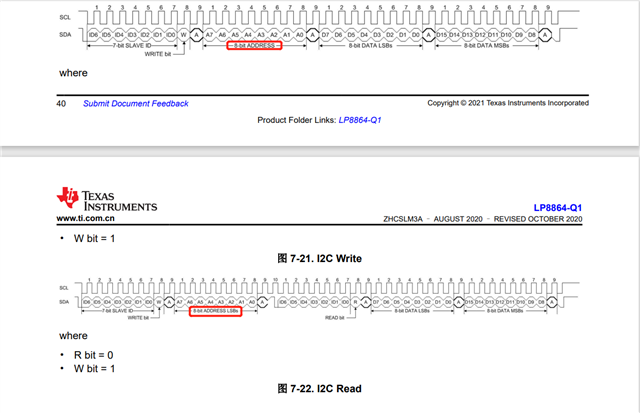
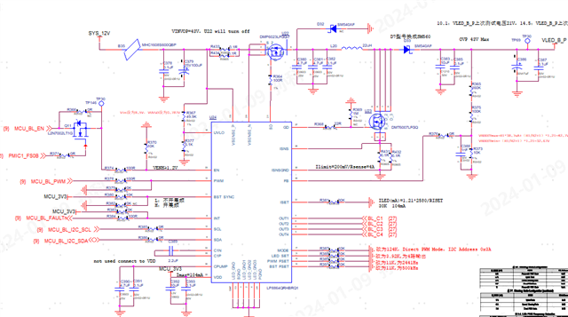
During the software debugging process, it was found that when using IIC to communicate with the backlight chip Lp8864, the data reading was normal, but the data writing was invalid. After investigation, it was found that during the second step of IIC communication (sending the register address to be written) when writing data, the backlight chip did not receive an ACK reply. However, when reading data (reading register data with the same address), during the second step of IIC communication (sending the register address to be read) when reading data, The backlight chip has an ACK response. Upon consulting the chip manual, it was found that the only difference between the first two steps of IIC communication, whether reading or writing data, is: The second step of reading data requires sending 8-bit ADDRESS LSBs The second step of writing data requires sending 8-bit ADDRESS The description of register address in the chip manual only includes offset address, but no description of register address is found. Therefore, I would like to ask if there is a difference in address when the chip reads and writes the same register?