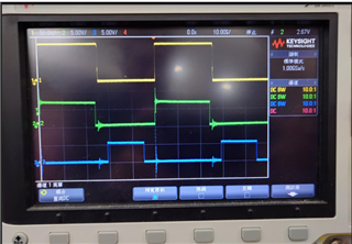
This thread has been locked.

If you have a related question, please click the "Ask a related question" button in the top right corner. The newly created question will be automatically linked to this question.

UCC21320-Q1: Gate signal issue

Part Number: UCC21320-Q1

Hi team,

Could you help check what issue caused the situation?  why does high output delay around 2us then turn to low? thanks 

Green is High side input

Red is High side output

Blue is low side input

Yellow is low side output
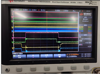
  • Hi Jimmy, 

    Is this observed behavior for a specific gate driver, or happens on all of the gate drivers? 

    From your waveform capture, since the red signal has 50V/div, is it the switch node signal or the output signal? Since the maximum output cannot reach ~100V, so I wonder if that's the bus voltage instead. 

    If it is indeed the switch node signal, that makes sense: the high side gate driver turns on, and switch node rises to ~100V; then both high side and low side drivers are off, switch node is at high-Z (which is why it remained high); then low side driver turns on, switch node voltage drops to 0. 

    I was also wondering what the yellow signal represents, since it shows 1V/div, so maximum is around ~1.5V, but you mentioned this is the low side output signal. 

    I looked at the schematic and nothing seems too alarming, besides the use of just a diode for turn-off. We recommend having both turn-on and turn-off resistors. For next step of debug, maybe you can try removing the diode and see if that makes any difference. 

    Thanks, 

    Vivian

  • Hi team,

    Customer resend the waveform.

    yellow is U phase waveform

    Green is high side input signal

    Blue is Low low-side input signal.

    You can see the U phase(yellow) lags than the green signal(High side signal)

    So RD sees that the upper arm driver signal lags behind the input signal around 1us.

    It's normal? RD suspects that it is caused by the internal behavior of the driver.


  • Hi Jimmy, 

    Several factors might cause this behavior: 

    1. Probe timing skew, as in the two probes' timing are not aligned correctly. The customer can hook these two probes to the same signal to check whether there's a timing difference between the two probes. 

    2. Propagation delay. UCC21320 has a maximum propagation delay of ~30ns. 

    3. Turn-on and turn-off speed of the power FET they're using. 

    I would recommend them to calibrate their probes, then to measure the input signal and the output signal (OUTA/OUTB) directly. Maybe even measure it without any load. This way, we can see the behavior of the gate driver without the influence of the system. 

    Please let me know what they find out based on this. Thanks! 

    Vivian

  • Hi team,

    If the customer uses low side GND to get High side output signal like below pic.

    Will this affect the output?  what do you think?

  • Hi Jimmy, 

    OUTA should be measured relative to VSSA instead of VSSB. They should use a differential probe, since VSSA is a floating ground. 

    Please advice the customer to measure the OUTA-VSSA signal with a differential probe, as well as measure OUTB-VSSB signal (can use passive probe for this measurement). 

    Thanks, 

    Vivian