


Hi team,
Could you please help review the schematic and give some comments? Many thanks.
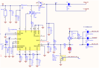
My customer controls LM51501-Q1 start-up via external triple switches OH_NO_SW, Terminal1 and IH_NO_SW.
When the LM51501-Q1 start-up, they press the switch to connect to GND, which turn on the PMOS, so that CE can enable EN PIN and wake up LM51501-Q1.
Then use the VOUT PIN of BOOST to continuously maintain the high voltage of EN.
After the entire system works normally, the MCU turns on the Q14 and pulls the EN down to a low level to shut down LM51501-Q1.
The three switches OH_NO_SW, Terminal1, IH_NO_SW are self-rebound switches and are open when normally be left. They are not grounded until they are pressed.
CE is a super capacitive voltage with a usable range of 2.1-2.8V and is also the input voltage for BOOST.
The output voltage after boost is set to 6.5V.
Regards,
Ivy