This thread has been locked.

If you have a related question, please click the "Ask a related question" button in the top right corner. The newly created question will be automatically linked to this question.

LM5164-Q1: Input power consumption while below UVLO threshold

Part Number: LM5164-Q1
Other Parts Discussed in Thread: LM5164, LM5169

Hello

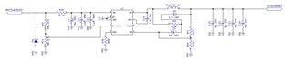
Im currently using the LM5164 to convert a 48v battery to 13v. While in the normal input voltage range, the input current consumption is around 800uA. However, when the input voltage drops below my 28V UVLO threshold, the output of the LM5164 drops to 2.4V and the input current increases to 1.4mA. In this state, the LM5164 becomes noticeably hotter. The EN/UVLO pin voltage is around 1V. 

any feedback would be appreciated, currently this circuit is unusable with this behavior. 

  • Hello

    Please provide your complete schematic.

    Also, please provide switching waveforms during normal and abnormal behavior.

    Thanks

  • when measuring the SW node, everything looks normal while in normal operation.  once the input is below the UVLO threshold, the SW node becomes a DC signal that settles to 2.5V.  this forum doesnt let me attach picture or PDF files, is there another way to share?

  • Hello

    You might try jpeg; you should be able to drag it into the text box.

    I assume you are looking at no load ?

    You may want to try it with some load.

    Thanks

  • this is load independent.  i really dont mind the SW node going to 2.5V.  the real problem is the input current increasing from 800uA to 1.4mA while below UVLO.  The datasheet dictates that the input current should be 10uA in this condition 

  • Hello

    The SW node should not sit at a D.C. level of 2.5V, unless there is some large leakage on that pin.

    Both the SW and Vout should gradually drop to zero when the device is disabled even with the FB divider load.

    Can you test with the 10Ω shorted out.

    I assume the 1V on the EN pin was measured with 20Vin ?

    I would like to be sure that the device functions with 28Vin or less.

    Can you remove the bottom EN resistor and make sure that you can regulate at less than 28Vin.

    Also, try using a voltage source on the EN input and make sure that the thresholds on that pin are correct

    and the function is correct.

    Have you tested more than one regulator sample ?

    Thanks

  • Hello Frank

    I agree that 2.5V on the SW node is very odd

    I shorted out the 10 Ohm input resistor (just there to prevent sparking upon connection). i did notice a decrease in input current consumption however i now get a jump from about 600uA above the UVLO to 1mA when below the UVLO...... still not 10uA

    yes 1V at the FB pin was about 20V at the input

    I removed the bottom UVLO/EN resistor and the device maintains 13V at the output with lower than 28V input (tested down to 18V)

    I can confirm that the jump in input current occurs when the feedback pin voltage is less than 1.4ish volts.  

    this behavior exists on all 5 of my samples as well as a few other projects that use this circuit. (i just never measured this)

    the device seems healthy as it will provide 300mA and barely get warm.  any other ideas?

    thank you again

  • Hello

    Are you measuring the input current at the VIN pin or at the "BATTsw" connector ?

    Try to measure at the 10Ω.

    It looks like we will have to test this out in our lab, since I don't see anything obvious.

    Thanks

  • i am measuring at the BATTsw connector but this circuit is the only this populated on the board at the moment.  i have ordered a demo board and plan to see if i can duplicate this when it arrives (hopefully tomorrow).  

  • Hello

    I will have our technician check this in the lab.

    Thanks

  • Hello 

    I purchased and EVM for this IC and ran the same test after removing the 1M R5 resistor from the board and applying a controlled voltage to the enable pin. 

    with Vin = 26V and UVLO/EN <= 0.7V, Vout = 0V and Iin = 10uA. 

    with Vin = 26V and UVLO/EN > 1.5V, Vout = 12.1V and Iin = 30uA

    with Vin = 26V and UVLO/EN between 0.7V and 1.5V, Vout = 2.2V and Iin = 580uA

    this mimics the behavior that I’ve been experiencing. I’m not sure what the point is in having an undervoltage lockout function if it draws almost 20x the no load operating current and the output stays partially active.

    is this what you have seen in your testing as well?

    thank you

  • Hello

    My technician is in the process of getting an EVM and will test as soon

    as possible.

    Thanks

  • Hello

    We confirm that the device is partially on when the EN input is between 0.7V and 1.5V.

    I will discuss this with our Design and Applications engineers and see if we can shed more light

    on this phenomenon.

    Thanks

  • Thank you

     were you able to see a big increase in input current when enable drops below 1.4V?

  • Hello

    Yes we see an increase in the input current in that region.

    Thanks

  • Hello

    If your load current is in the 600mA range, you may want to look at the LM5169 family.

    That device does not exhibit the same input current phenomenon as the LM5164

    Thanks

  • Hello

    Ill take that into consideration however i need to know if this is a design intent behavior (which i doubt) or if this is a systemic issue or part defect.  marketing this device for battery powered systems is pretty dangerous considering the implications of this behavior.  We've had a few field reports of 48V battery modules discharging well past the safe voltage limits in a unreasonably short period of time.   has TI engineering weighed in on this issue?

    thank you again

  • Hello

    We are following up with our design team about your questions.

    Thank you for your patience.

    We hope to get back to you later this week.

    Thanks

  • Hello 

    has there been any new updates on this? Is this part behavior a systematic design issue? Could this be a sign of a larger problem? I’m debating whether or not to drop this component for new designs or add additional circuitry to bandaid the issue. Or is this going to be fixed in later production runs?

    thank you

    andrew

  • Hello

    We have confirmed with our Designers that the behavior you are seeing is normal for this device.

    You may want to investigate another product that fits your requirements.

    Keep in mind that most of our data sheets do not specify, nor ensure, performance when operating

    in this "gray" zone of EN thresholds.  It is best to test any specific device to ensure that it will meet all 

    of your requirements before committing the design to production.

    Thanks