This thread has been locked.
If you have a related question, please click the "Ask a related question" button in the top right corner. The newly created question will be automatically linked to this question.
Hello,
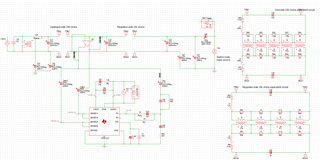
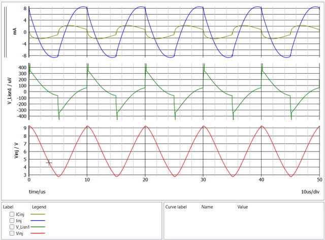
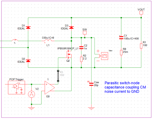
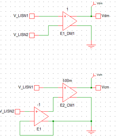
I believe that this a question for Timothy Hegarty. I am trying to use SIMPLIS model for TPSF12C1 (TPSF12C1-Q1 single-phase AEF circuit.sxsch) in more realistic circuit which includes LISN, Line impedance and PFC stage, but this IC does not work. Unfortunately I cannot attach my simulation file to this message. It looks as IC voltage saturated to Vdd. But increases of Vdd does not help. I am using all components from your original circuit. When I investigated your original file it also shows strange behaviour. When I placed voltage controlled voltage source between the lines and Csen1 & Csen2 (E2 enabled , R1 & R2 disabled )this IC does not work even all signals absolutely the same as in original circuit (E2 disabled, R1 & R2 enabled) See pic below. Could you, please, help with this problem. Also can PSPICE encrypted model for this IC work with Simetrix?
Regards.
Lev
Hi Lev,
The VCVS as connected in the schematic above will not allow current injection. Also, depending on the amplitude of the applied CM excitation (Vsw) through capacitor Csw that sets up a CM noise source current, the CM voltage disturbance at the filter center node (between the chokes, sensed by the AEF circuit) may be too high, thus causing saturation of the INJ pin voltage from a large-signal standpoint. You can check this with the TPSF12C1/3 quickstart calculator - just make sure the correct choke parameters are entered. Also, check the time-domain waveform in the simulation.
I attached a file with a 50uH LISN and show some results below. This file has a simpler choke model that corresponds to the Wurth 2mH choke in our single-phase filter EVM. Three series RL stages is typically enough to obtain a satisfactory behavioral model for the impedance profile of a nanocrystalline choke. Note Csw in this design is only 20pF, as the first stage of filtering is somewhat limited given the 2.2nF regulator-side Y-caps. Increase these Y-caps from 2.2nF to 4.7-10nF (while still meeting the touch current spec) to reduce the CM disturbance sensed by the AEF circuit, especially if the switching frequency is less than 100kHz.
PS: Note you can use Plot -> Fourier... menu in SIMPLIS to get a Fourier result of the LISN voltage, e.g. with AEF enabled/disabled. I increased the time duration from the normal 50µs to 250µs to get a higher res Fourier result, hence the slightly longer simulation run time.
Regards,
Tim
TPSF12C1EVM-FILTER AEF circuit with LISN.sxsch
Hi Tim,
Thank you very much for such a quick respond! The circuit you sent me has much more useful information. And this is exactly what I want to do: measure Fourier results on the LISN. But when I ran your circuit with AEF enabled/disabled I did not see any difference. This is because middle point of LISN must be connected to the Earth. When I did this, everything was working fine. AEF shows up to 45dB noise reduction. The next step I would suggest is to connect PFC output stage to this circuit. I believe that your customers would love this.
Regards,
Lev
Thanks Tim. If it is possible, could you, please, let me know when you add PFC.
Regards. Lev
lev.nemets@setec.com.au
Thanks, Lev. I will notify you when it's available. Are you using a totem-pole PFC topology? What is the power level and how many interleaved phases?
Regards,
Tim
Hi Tim,
Because all our current products are less than 1kW we are currently using single phase CCM PFC and interleave CrCM PFC. But my question about Active filter is general question. I hope that you can develop a simulation circuit as a template in which should have three connectors (Line, Neutral and Protecting Earth) were your customers could connect their PFC circuits. My problem with your current circuit that if I connect PFC power stage instead of noise source (Vsw) everything is OK. But I if connect PFC stage as in real circuit through a Bridge and inject CM noise by connecting MOSFET drain to protecting earth through Csw, the IC does not work
Regards
Lev
Thanks, Lev.
Send on your SIMPLIS file so I can take a look. Note that the GND of the PFC stage is typically not chassis GND (i.e. GND of the EMI filter).
Regards,
Tim
Hi Tim,
Thank you very much for supporting me. I placed the links to these files on Microsoft OneDrive and Google Drive. I hope you can access it. If no, please let me know how I can send it as TI page does not have attachment options.
Regards
Lev
lev.nemets@setec.com.au
https://drive.google.com/file/d/13_QTOmYvxVVurjKhQ2J85ifLmCuzRkfP/view?usp=sharing
https://drive.google.com/file/d/1JePVMZqSLlIZsV2yHtWs8sdIGeRT0_L6/view?usp=sharing
Hi Lev, I can't access those external drives. you should be able to drag the file into the message window to attach it.
--
Tim
Hi Tim,
Sorry for trouble. This webpage does not allow to drag and drop Simeterx files. It just shows download process and then nothing in the message window. So I Zipped these two files and now I can drag it into message.
Hope this time it will work.
Regards,
Lev
Hi Lev,
I edited the first SIMPLIS file you sent such that the boost DC/DC stage takes its input from the 120V supply connected to the LISN and the switch node injects capacitively into the GND node, which intuitively corresponds to a practical scenario. Note that the switch node has high dv/dt here, hence the large inject current spikes, LISN noise voltage, etc.
Aside from the bridge rectifier (which I haven't tried to add yet), this seems to be the circuit you requested. Ultimately, we can add a PFC control loop and and verify correct operation over a full AC line cycle.
0181.TPSF12C1 for TI rev2.sxsch
Regards,
Tim
Hi Lev, I think I accidentally deleted your post when I was replying. I'm glad to hear your file is working. If possible, please attach your version with the bridge rectifier attached.
Regards,
Tim
Hi Lev,
I made some minor edits to the file -- see attached. The switch node falling dv/dt is still a bit high, but that can be adjusted with MOSFET choice, snubber optimization, etc.
TPSF12C1EVM-FILTER with added boost stage.sxsch
Regards,
Tim
Hi Lev,
Here is an updated SIMPLIS file with a totem-pole (TTPL) setup running open loop at 50% duty cycle giving a 400V DC bus. This file extracts the DM and CM components of the total noise at the LISNs and includes a discrete inductor, L2 = 220uH, for DM filtering along with the X caps.
2768.TPSF12C1EVM-FILTER with TTPL boost stage.sxsch
Regards,
Tim
Hello Tim. Many thanks for the help. To complete this question, the value of E1_DM1 should be 0.5. That's my fault. Regards. Lev
Hi Lev,
Actually, a common definition of Vdm is V1 - V2, simply the difference in voltage, whereas Vcm is the average of the two voltages. I think it's fine as is.
Regards,
Tim