This thread has been locked.

If you have a related question, please click the "Ask a related question" button in the top right corner. The newly created question will be automatically linked to this question.

LMR36503-Q1: Switching node voltage undershoots abs max ratings from datasheet

Part Number: LMR36503-Q1
Other Parts Discussed in Thread: LMR36503, TPS62825, LM25148-Q1

Team,

A customer of mine is currently verifying their LMR36503 design. Can you please help with following question?

On a LMR36503 design we measure up to -0.63V at the switching node: 


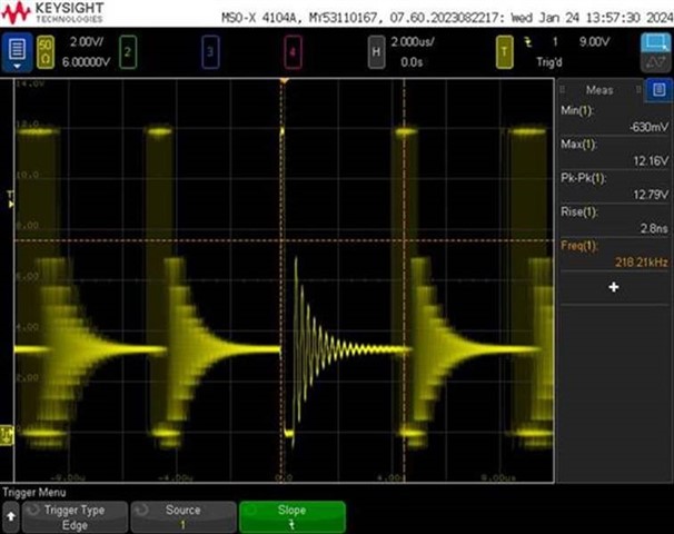
For me this looks like a quite normal behavior of the DC/DC: When the bottom FET turns off, the current continues flowing through the inductor and for a moment the current flows through the bulk diode of the integrated bottom FET. This current causes a negative voltage of about 0.7V at the switching node.

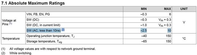
Here the relevant part of the datasheet:


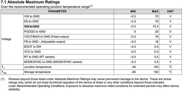
The voltage of -0.63V is beyond the absolute max ratings. Is there an additional information for this value, paying attention to transients during switching?

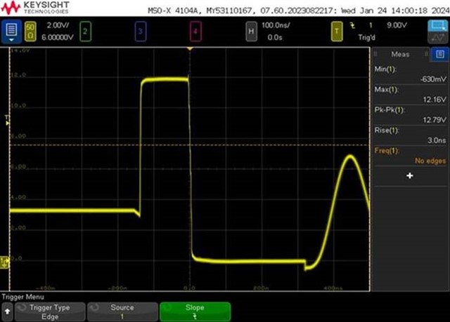
Here a good example of another DC/DC controller (TPS62825)


Do you think this waveform can be considered as OK or might there be a problem?


 They see similar behavior in a a LM25148-Q1 design. 

 Thanks,
  Robert

  • Hi Robert,

    This is normal operation and does not damage the part and your understanding is correct. -0.63V is caused by the output inductor driving current through a MOSFET body diode during switching operation. The minimum voltage rating found in the data sheet is actually a dc rating and means that the part could be damaged if a constant voltage below –0.3 V is applied at the SW node from a source other than the output inductor during switching operation.

    You can also refer to this application note for more details on the absolute Maximum Ratings of the SW node. Here is the Link.

    Regards,

    Hongjia