This thread has been locked.

If you have a related question, please click the "Ask a related question" button in the top right corner. The newly created question will be automatically linked to this question.

LMR16030: Webench selection for D1

Guru 54428 points
Part Number: LMR16030

Hello,

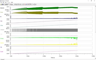
Oddly the Tina exported encrypted model produces cathode current greater than the device being selected for 2.5A output at 48v input bucked +24v. Webench edit function select alternative diode does not come close to  Nexperian PMEG6045ETP producing greater efficiency and handle cathode current Tina analysis shows in excess of 3.5A. Judging efficiency and robustness by the PMEG6045ETP lower forward drop and much higher cathode current as the high side NFET should shut down under protection control by UVLO recovery or even a reset condition.

Why is the Tina model selecting a lower cathode current and twice the blocking voltage when the input voltage should never be seen at the cathode of the switching diode?

Opinion being diode or fuse should short/blow when such a serious condition should ever arise. Worst case scenario we have to replace an inline fuse, not the MCU and several other switching regulators. Note the forward voltage drop 4.5mV of the PMEG6045ETP produces less stress on the diode and high side NFET. Seemingly Webench should come close to selecting similar diode but never allows Tina analysis, why is that? Nexperian has done excellent Schottky diode testing at turtle speeds 300µs worst case scenario seems evident.

IF = 3 A; tp ≤ 300 µs; δ ≤ 0.02; Tj = 25 °C; pulsed - 420 475 mV

IF = 4 A; tp ≤ 300 µs; δ ≤ 0.02; Tj = 25 °C; pulsed - 450 510 mV

IF = 4.5 A; tp ≤ 300 µs; δ ≤ 0.02; Tj = 25 °C; pulsed - 460 530 mV

Webench_LMR16030SDDA 38v-54v-24vout.tscDiode Schottky 60v 4.5amp SOD128 PMEG6045ETP Nexperia.pdf

  • Hello Genato,

    I didn't get your saying about: “when the input voltage should never be seen at the cathode of the switching diode?”

    when high side NFET  turn on, the amplitude of SW is Vin, this voltage will seen on cathode of the switching diode.

    So it need choose higher blocking voltage than Vin, but I think twice of Vin_max is too conservative, it is ok to choose 1.2Vin_max. And cathode current should be large than 1.2*Iout_max.

    When these conditions are met, we can choose a diode with a smaller forward voltage drop. This is very flexible and does not have to completely refer to the recommendations of TINA or webench.

    Thanks

    Colin

  • Hello Colin,

    when high side NFET  turn on, the amplitude of SW is Vin, this voltage will seen on cathode of the switching diode.

    Perhaps you mean to say NFET drain this case +48v. Though NFET source PWM magnitude is very near desired output voltage 24v. The FB loop keeps full input supply from cathode of diode, roughly +24v smoothed out by the inductor and output caps. Tina transient analysis confirms but my question is how to simulate NXP diode as it does not exist as an alternative?

    The LMR16030 encrypted macro holds the diode properties. So a customer cannot input specific diode forward voltage drop, rated current, PRV values. The list of alternative diodes is excessive or way under current for this simple design. The export downloaded diode with lower current than switching peak load 2.5A will end in disaster there is no safety margin a 3.5 amp diode would be next best choice.

    The 4.5A 60v diode does not exist in the list of alternatives for macro export, can TI support please add NXP data. In reality the only time the diode might see 60v is UVLO recovery, in that case it should blow an inline fuse after diode shorts to protect downstream circuits. Past older theory suggested high PRV diode as reverse current from the inductor EMF goes to ground in buck designs. The faster switching speeds 760KHz seemingly reduces inductive EMF into cathode reduces reverse current to ground. Tina analysis macro does not show the inductors EMF reverse current to ground through the diode. Seemingly we could under rate the PRV 50v for protective counter measure since the buck down output peaks 24v. An alternative is overshoot control built into the switcher or 30-40v Zener diode on the +24v output. So adding reverse current for the inductor or diode into the macro could help the customer.  

  • Hello Genatco,

    I am not very familiar with TINA, but you can use pspice for TI to simulate this situation. I know psipce can add the parameters of diode. 

    B R

    Colin

  • Hi Collin, 

    The webench exported macro transient analysis incorrectly plots 48v on the inductor input VSwitch L1. The switched inductor does not isolate input supply voltage at the NFET source as the FB control bucks down 24v. LMR control fold back loop regulates NFET source voltage via PWM pulse width. Seemingly If there was anywhere close to 48v on the inductor it would pass to the output capacitors. I could believe pulses being 26-28v, never 48v P2P as L1 being 15µH basically a short piece of coiled wire wound on a ferrite bobbin. Be interesting to see the real device switching on oscilloscope probe capture, would be more believable. The 100KHz buck regulators we designed around 1985 had PN or NPN saturated switches, TIP42B, TIP41C were very efficient for the time bucked +36v down to +12v +5v.

    Diode 3.6A graph is seemingly shorting out rated current for the diode selected being tested often by single halfwave so many microseconds long.

  • Hi Sir,

    We advise you using pspice for further check.
    I think WEBENCH does not have device level simulation capabilities.

    Colin

  • Agree Webench macro export feature needs to be fixed so the NFET shows any VDS drop from PWM regulation on input of inductor from FB loop control.