This thread has been locked.

If you have a related question, please click the "Ask a related question" button in the top right corner. The newly created question will be automatically linked to this question.

BQ78350: BQ78350 little endian query

Part Number: BQ78350
Other Parts Discussed in Thread: BQSTUDIO

Hi 

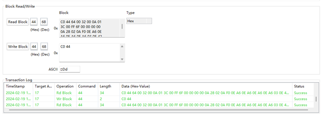
The customer test with BQ78350, The protection parameters seem are not  little endian data. 

For example, 0x44CC is 0x0A and 0x44CE is 0x28. The CUV voltage is 2600. If the LSB is first, 0x28A0 is not 2600, but 10250, and 0x0A28 is exactly 2600. I have verified the same of other subsequent data.

Please help check it.

Thanks

Star

  • Hello star,

    Can you share some screen captures of the logic analyzer data showing big endian? Or what you are inputting/reading from the BQStudio advanced communication tab?

    This is only with the protection data?

    Sincerely,

    Wyatt Keller

  • Hi Wyatt

    Thanks for your reply.

    The field of CUV threshold is 0x0A 0x28. It is found that only the protection data is like this.

    Waiting for your reply.

    Thanks 

    Star

  • Hey Star,

    Today's a federal holiday so no one is in the office. We will get back to you tomorrow.

    Regards,
    Nick Richards

  • Hello Star,

    Can you share the .gg file also so I can see which firmware version you are using? I have been reviewing your screenshot, but the screenshot is showing the CTO and OC protections if I look at the BQ78350 TRM, so I assume it is a different firmware version. Can you also verify the correct BQZ file is being used for the gauge being read from? There could be memory mapping differences between different firmware versions which would show up as memory.

    Sincerely,

    Wyatt Keller

  • Hi Wyatt

    Thanks for your reply.

    Attached the .gg file for your reference.

    * Texas Instruments Data Flash File
    * File created Thu Feb 22 16:49:25 2024
    *
    * Device Number 1E9B
    * Firmware Version 2.02
    * Build Number 28
    * Order Number 0
    *
    * bqz Device Number 1E9B
    * bqz Firmware Version 2.02
    * bqz Build Number 28
    *
    * Field Order: Class name  SubClass name  Parameter name  Parameter Value  Display Units  Data Type  Data Length  Address Offset  Default Value  Minimum Value  Maximum Value  Display Format  Read Formula  Write Formula  Flags  Help  Native Units  Data Flash Raw Value
    Calibration Current CC Gain 0.65 mOhm F 4 0 1 1.00E-01 9.00E+00 ff.fff 8.4381/x 8.4381/x - 0x844fcace
    Calibration Current Capacity Gain 0.65 mOhm F 4 4 1 2.98E+04 2.69E+07 ff.fff 2517328.05/x 2517328.05/x - 0x966c6bde
    Calibration Voltage Cell1 Offset 0 mV I 1 8 0 -128 127 ddd x+0 x mV 0x00
    Calibration Voltage Cell2 Offset 0 mV I 1 9 0 -128 127 ddd x+0 x mV 0x00
    Calibration Voltage Cell3 Offset 0 mV I 1 10 0 -128 127 ddd x+0 x mV 0x00
    Calibration Voltage Cell4 Offset 0 mV I 1 11 0 -128 127 ddd x+0 x mV 0x00
    Calibration Voltage Cell5 Offset 0 mV I 1 12 0 -128 127 ddd x+0 x mV 0x00
    Calibration Voltage Cell6 Offset 0 mV I 1 13 0 -128 127 ddd x+0 x mV 0x00
    Calibration Voltage Cell7 Offset 0 mV I 1 14 0 -128 127 ddd x+0 x mV 0x00
    Calibration Voltage Cell8 Offset 0 mV I 1 15 0 -128 127 ddd x+0 x mV 0x00
    Calibration Voltage Cell9 Offset 0 mV I 1 16 0 -128 127 ddd x+0 x mV 0x00
    Calibration Voltage Cell10 Offset 0 mV I 1 17 0 -128 127 ddd x+0 x mV 0x00
    Calibration Voltage Cell11 Offset 0 mV I 1 18 0 -128 127 ddd x+0 x mV 0x00
    Calibration Voltage Cell12 Offset 0 mV I 1 19 0 -128 127 ddd x+0 x mV 0x00
    Calibration Voltage Cell13 Offset 0 mV I 1 20 0 -128 127 ddd x+0 x mV 0x00
    Calibration Voltage Cell14 Offset 0 mV I 1 21 0 -128 127 ddd x+0 x mV 0x00
    Calibration Voltage Cell15 Offset 0 mV I 1 22 0 -128 127 ddd x+0 x mV 0x00
    Calibration Current Offset CC Offset 0 - I 2 24 0 -32767 32767 ddddd x+0 x - 0x0000
    Calibration Current Offset Coulomb Counter Offset Samples 64 - U 2 26 64 0 65535 dddd x+0 x - 0x0040
    Calibration Temperature T1 Temp Offset 0 degC I 1 30 0 -128 127 dd.d x+0 x 0.1degC 0x00
    Calibration Temperature T2 Temp Offset 0 degC I 1 31 0 -128 127 dd.d x+0 x 0.1degC 0x00
    Calibration Temperature T3 Temp Offset 0 degC I 1 32 0 -128 127 dd.d x+0 x 0.1degC 0x00
    Calibration Temperature Gauge Internal Temp Offset 0 degC I 1 33 0 -128 127 dd.d x+0 x 0.1degC 0x00
    Calibration Ext Cell Voltage Ext Cell Divider Gain 4653 - I 2 34 5000 0 32767 dddd x+0 x - 0x122d
    Calibration VAux Voltage VAux Gain 37834 - I 4 36 5000 0 100000 dddddddd x+0 x - 0x000093ca
    Calibration Cell Temperature Model Coeff a1 -11130 - I 2 1373 -11130 -32768 32767 ddddd x+0 x - 0xd486
    Calibration Cell Temperature Model Coeff a2 19142 - I 2 1375 19142 -32768 32767 ddddd x+0 x - 0x4ac6
    Calibration Cell Temperature Model Coeff a3 -19262 - I 2 1377 -19262 -32768 32767 ddddd x+0 x - 0xb4c2
    Calibration Cell Temperature Model Coeff a4 28203 - I 2 1379 28203 -32768 32767 ddddd x+0 x - 0x6e2b
    Calibration Cell Temperature Model Coeff a5 892 - I 2 1381 892 -32768 32767 ddddd x+0 x - 0x037c
    Calibration Cell Temperature Model Coeff b1 328 - I 2 1383 328 -32768 32767 ddddd x+0 x - 0x0148
    Calibration Cell Temperature Model Coeff b2 -605 - I 2 1385 -605 -32768 32767 ddddd x+0 x - 0xfda3
    Calibration Cell Temperature Model Coeff b3 -2443 - I 2 1387 -2443 -32768 32767 ddddd x+0 x - 0xf675
    Calibration Cell Temperature Model Coeff b4 4696 - I 2 1389 4696 -32768 32767 ddddd x+0 x - 0x1258
    Calibration Cell Temperature Model Rc0 11703 - I 2 1391 11703 -32768 32767 ddddd x+0 x - 0x2db7
    Calibration Cell Temperature Model Adc0 11703 - I 2 1393 11703 -32768 32767 ddddd x+0 x - 0x2db7
    Calibration Fet Temperature Model Coeff a1 -11130 - I 2 1399 -11130 -32768 32767 ddddd x+0 x - 0xd486
    Calibration Fet Temperature Model Coeff a2 19142 - I 2 1401 19142 -32768 32767 ddddd x+0 x - 0x4ac6
    Calibration Fet Temperature Model Coeff a3 -19262 - I 2 1403 -19262 -32768 32767 ddddd x+0 x - 0xb4c2
    Calibration Fet Temperature Model Coeff a4 28203 - I 2 1405 28203 -32768 32767 ddddd x+0 x - 0x6e2b
    Calibration Fet Temperature Model Coeff a5 892 - I 2 1407 892 -32768 32767 ddddd x+0 x - 0x037c
    Calibration Fet Temperature Model Coeff b1 328 - I 2 1409 328 -32768 32767 ddddd x+0 x - 0x0148
    Calibration Fet Temperature Model Coeff b2 -605 - I 2 1411 -605 -32768 32767 ddddd x+0 x - 0xfda3
    Calibration Fet Temperature Model Coeff b3 -2443 - I 2 1413 -2443 -32768 32767 ddddd x+0 x - 0xf675
    Calibration Fet Temperature Model Coeff b4 4696 - I 2 1415 4696 -32768 32767 ddddd x+0 x - 0x1258
    Calibration Fet Temperature Model Rc0 11703 - I 2 1417 11703 -32768 32767 ddddd x+0 x - 0x2db7
    Calibration Fet Temperature Model Adc0 11703 - I 2 1419 11703 -32768 32767 ddddd x+0 x - 0x2db7
    Calibration Fet Temperature Model Rpad 0 - I 2 1421 0 -32768 32767 ddddd x+0 x - 0x0000
    Calibration Fet Temperature Model Rint 18000 - I 2 1423 18000 -32768 32767 ddddd x+0 x - 0x4650
    Calibration Current Deadband Deadband 3 mA U 1 792 3 0 255 ddd x+0 x mA 0x03
    Calibration Current Deadband Coulomb Counter Deadband 38 264nV U 1 793 38 0 255 ddd x+0 x 264nV 0x26
    Settings Protection Protection Configuration 0 hex B 1 1223 0 0 0x7e hh x x RSVD|DIS_AFE_TIME_RECOV|CC_DSG_OFF|DC_CHG_OFF|LPEN|VAUXR|CUV_RECOV_CHG|RSVD hex 0x00
    Settings Protection Enabled Protections A ff hex U 1 1224 ff 0 0xff hh x x ASCDL|ASCD|AOLDL|AOLD|OCD|OCC|COV|CUV hex 0xff
    Settings Protection Enabled Protections B 6f hex U 1 1225 7f 0 0x7f hh x x RSVD|OCDL|OTF|AFE_OVRD|UTD|UTC|OTD|OTC hex 0x6f
    Settings Protection Enabled Protections C 0 hex U 1 1226 15 0 0x1f hh x x RSVD|RSVD|RSVD|OC|RSVD|CTO|RSVD|PTO hex 0x00
    Settings Protection Enabled Removal Recovery A 0 hex U 1 1228 0 0 0xfc hh x x ASCDL|ASCD|AOLDL|AOLD|OCD|OCC|RSVD|RSVD hex 0x00
    Settings Protection Enabled Removal Recovery B 0 hex U 1 1229 0 0 0x40 hh x x RSVD|OCDL|RSVD|RSVD|RSVD|RSVD|RSVD|RSVD hex 0x00
    Settings Permanent Failure Enabled PF A 0 hex U 1 1323 0 0 0xff hh x x DFETF|CFETF|VIMR|SOT|SOCD|SOCC|RSVD|RSVD hex 0x00
    Settings Permanent Failure Enabled PF B 0 hex U 1 1324 0 0 0xff hh x x SOTF|TS3|TS2|TS1|AFE_XRDY|AFE_OVRD|AFEC|AFER hex 0x00
    Settings Configuration Temperature Enable 0f hex B 1 1195 9 0 0x1f hh x x RSVD|RSVD|RSVD|RSVD|Source|TS3|TS2|TS1 hex 0x0f
    Settings Configuration Temperature Mode 4 hex B 1 1196 0 0 0x07 hh x x RSVD|RSVD|RSVD|RSVD|RSVD|TS3 Mode|TS2 Mode|TS1 Mode hex 0x04
    Settings Configuration DA Configuration 19 hex B 1 1197 11 0 0xdf hh x x FTEMP|CTEMP|RSVD|VEXTAVG_EN|VAUX_EN|VAUX_SCALE|IN_SYSTEM_SLEEP|SLEEP hex 0x19
    Settings Configuration AFE Cell Map 7fff hex B 2 1198 13 0 0x7fff hhhh x x RSVD|CELL_15|CELL_14|CELL_13|CELL_12|CELL_11|CELL_10|CELL_9|CELL_8|CELL_7|CELL_6|CELL_5|CELL_4|CELL_3|CELL_2|CELL_1 hex 0x7fff
    Settings Configuration FET Options 44 hex B 2 1119 21 0 0x0fff hhhh x x RSVD|RSVD|RSVD|RSVD|PDSG_POL|PDSG_EN|KEY_POL|PCHG_POL|RSVD|SLEEPCHG|CHGFET|CHGIN|CHGSU|OTFET|KEY_EN|PCHG_EN hex 0x0044
    Settings Configuration Sbs Gauging Configuration 2 hex B 1 1121 0 0 0x83 hh x x PWRMSleep|RSVD|RSVD|RSVD|RSVD|RSVD|RSOC_HOLD|RSOCL hex 0x02
    Settings Configuration Smb Configuration a0 hex B 1 1122 a0 0 0xb7 hh x x FIXED_ADDR|RSVD|BLT1|BLT0|RSVD|HPE|CPE|BCAST hex 0xa0
    Settings Configuration Power Config 0 hex B 1 1138 0 0 0x01 hh x x RSVD|RSVD|RSVD|RSVD|RSVD|RSVD|RSVD|AUTO_SHIP_EN hex 0x00
    Settings Configuration LED Configuration 0 hex B 1 1166 0 0 0xff hh x x RSVD|RSVD|LCD_SLEEP_DIS|LCDEN|LEDMODE|LEDCHG|LEDRCA|LEDR hex 0x00
    Settings Configuration SOC Flag Config 02fb hex B 2 1506 02fb 0 0x13ff hhhh x x RSVD|RSVD|RSVD|SBS_COMP|RSVD|RSVD|FCCLEARRSOC|FCSETRSOC|FDCLEARRSOC|FDSETRSOC|TCSETVCT|FCSETVCT|TCCLEARRSOC|TCSETRSOC|TDCLEARRSOC|TDSETRSOC hex 0x02fb
    Settings Configuration Balancing Configuration 1 hex B 1 1599 1 0 0xff hh x x RSVD|RSVD|RSVD|RSVD|RSVD|RSVD|RSVD|CB hex 0x01
    Settings Configuration CEDV Gauging Configuration 26 hex B 2 1433 2 0 0x7ff hhhh x x RSVD|RSVD|RSVD|RSVD|RSVD|FC_FOR_VDQ|RSVD|FCC_LIMIT|VFLT_EN|RSVD|FIXED_EDV0|SC|EDV_CMP|EDV_EXT_CELL|CSYNC|CCT hex 0x0026
    Settings Fuse PF SAFE A 0 hex U 1 1112 0 0 0xff hh x x DFETF|CFETF|VIMR|SOT|SOCD|SOCC|SOV|SUV hex 0x00
    Settings Fuse PF SAFE B 0 hex U 1 1113 0 0 0xff hh x x SOTF|TS3|TS2|TS1|AFE_XRDY|AFE_OVRD|AFEC|AFER hex 0x00
    Settings Fuse PF SAFE C 0 hex U 1 1114 0 0 0x03 hh x x RSVD|RSVD|RSVD|RSVD|RSVD|RSVD|DFW|IFC hex 0x00
    Settings Fuse Fuse Blow Timeout 30 s U 1 1118 30 0 255 ddd x+0 x s 0x1e
    Settings Aux SMB Address Addr Reads 3 - U 1 1123 3 0 10 ddd x+0 x - 0x03
    Settings Aux SMB Address SMBTAR_ADDR0 20 hex U 1 1124 20 0 0xff hh x x hex 0x20
    Settings Aux SMB Address SMBTAR_ADDR1 22 hex U 1 1125 22 0 0xff hh x x hex 0x22
    Settings Aux SMB Address SMBTAR_ADDR2 24 hex U 1 1126 24 0 0xff hh x x hex 0x24
    Settings Aux SMB Address SMBTAR_ADDR3 25 hex U 1 1127 25 0 0xff hh x x hex 0x25
    Settings Aux SMB Address SMBTAR_ADDR4 26 hex U 1 1128 26 0 0xff hh x x hex 0x26
    Settings Aux SMB Address SMBTAR_ADDR5 28 hex U 1 1129 28 0 0xff hh x x hex 0x28
    Settings Aux SMB Address SMBTAR_ADDR6 2a hex U 1 1130 2a 0 0xff hh x x hex 0x2a
    Settings Aux SMB Address SMBTAR_ADDR7 2c hex U 1 1131 2c 0 0xff hh x x hex 0x2c
    Settings SMB Master Mode Host Address 10 hex U 1 1134 10 0 0xff hh x x hex 0x10
    Settings SMB Master Mode Charger Address 12 hex U 1 1135 12 0 0xff hh x x hex 0x12
    Settings SMB Master Mode Alarm Timer 10 s U 1 1136 10 10 255 ddd x+0 x s 0x0a
    Settings SMB Master Mode Charger Request Timer 50 s U 1 1137 50 10 255 ddd x+0 x s 0x32
    Settings Manufacturing Mfg Status init 00b0 hex B 2 712 0 0 0xffff hhhh x x RSVD|RSVD|RSVD|RSVD|RSVD|RSVD|LED_EN|SAFE_EN|BBR_EN|PF_EN|LF_EN|FET_EN|RSVD|RSVD|RSVD|RSVD hex 0x00b0
    Protections CUV Threshold 2500 mV I 2 1230 2500 0 32767 dddd x+0 x mV 0x09c4
    Protections CUV Delay 2 s U 1 1232 2 0 255 ddd x+0 x s 0x02
    Protections CUV Recovery 2600 mV I 2 1233 3000 0 32767 dddd x+0 x mV 0x0a28
    Protections COV Threshold Low Temp 3650 mV I 2 1235 4300 0 32767 ddd x+0 x mV 0x0e42
    Protections COV Threshold Standard Temp 3650 mV I 2 1237 4300 0 32767 ddd x+0 x mV 0x0e42
    Protections COV Threshold High Temp 3650 mV I 2 1239 4300 0 32767 ddd x+0 x mV 0x0e42
    Protections COV Threshold Rec Temp 3650 mV I 2 1241 4300 0 32767 ddd x+0 x mV 0x0e42
    Protections COV Delay 3 s U 1 1243 2 0 255 ddd x+0 x s 0x03
    Protections COV Recovery Low Temp 3550 mV I 2 1244 3900 0 32767 ddd x+0 x mV 0x0dde
    Protections COV Recovery Standard Temp 3550 mV I 2 1246 3900 0 32767 ddd x+0 x mV 0x0dde
    Protections COV Recovery High Temp 3550 mV I 2 1248 3900 0 32767 ddd x+0 x mV 0x0dde
    Protections COV Recovery Rec Temp 3550 mV I 2 1250 3900 0 32767 ddd x+0 x mV 0x0dde
    Protections OCC Threshold 11000 mA I 2 1252 6000 -32768 32767 dddd x+0 x mA 0x2af8
    Protections OCC Delay 1 s U 1 1254 6 0 255 ddd x+0 x s 0x01
    Protections OCC Recovery Threshold 40 mA I 2 1255 -200 -32768 32767 dddd x+0 x mA 0x0028
    Protections OCC Recovery Delay 30 s U 1 1257 5 0 255 ddd x+0 x s 0x1e
    Protections OCD Threshold -13000 mA I 2 1258 -6000 -32768 32767 dddd x+0 x mA 0xcd38
    Protections OCD Delay 10 s U 1 1260 6 0 255 ddd x+0 x s 0x0a
    Protections OCD Recovery Threshold -300 mA I 2 1261 200 -32768 32767 dddd x+0 x mA 0xfed4
    Protections OCD Recovery Delay 30 s U 1 1263 5 0 255 ddd x+0 x s 0x1e
    Protections OCDL Latch Limit 5 - U 1 1264 5 0 255 ddd x+0 x - 0x05
    Protections OCDL Counter Dec Delay 10 s U 1 1265 10 0 255 ddd x+0 x s 0x0a
    Protections OCDL Reset 30 s U 1 1266 15 0 255 ddd x+0 x s 0x1e
    Protections AOLD Latch Limit 5 - U 1 1267 0 0 255 ddd x+0 x - 0x05
    Protections AOLD Counter Dec Delay 10 s U 1 1268 10 0 255 ddd x+0 x s 0x0a
    Protections AOLD Recovery 5 s U 1 1269 5 0 255 ddd x+0 x s 0x05
    Protections AOLD Reset 30 s U 1 1270 15 0 255 ddd x+0 x s 0x1e
    Protections AOLD Threshold and Delay 1f hex U 1 1203 0 0 0xff hh x x RSVD|OCD_D2|OCD_D1|OCD_D0|OCD_T3|OCD_T2|OCD_T1|OCD_T0 hex 0x1f
    Protections ASCD Latch Limit 3 - U 1 1271 0 0 255 ddd x+0 x - 0x03
    Protections ASCD Counter Dec Delay 10 s U 1 1272 10 0 255 ddd x+0 x s 0x0a
    Protections ASCD Recovery 5 s U 1 1273 5 0 255 ddd x+0 x s 0x05
    Protections ASCD Reset 15 s U 1 1274 15 0 255 ddd x+0 x s 0x0f
    Protections ASCD Threshold and Delay 1f hex U 1 1202 0 0 0xff hh x x RSNS|RSVD|RSVD|SCD_D1|SCD_D0|SCD_T2|SCD_T1|SCD_T0 hex 0x1f
    Protections OTC Threshold 65 1degC I 2 1275 55 -400 1500 ddd.d x+0 x 0.1degC 0x028a
    Protections OTC Delay 2 s U 1 1277 2 0 255 ddd x+0 x s 0x02
    Protections OTC Recovery 60 1degC I 2 1278 50 -400 1500 ddd.d x+0 x 0.1degC 0x0258
    Protections OTD Threshold 65 1degC I 2 1280 60 -400 1500 ddd.d x+0 x 0.1degC 0x028a
    Protections OTD Delay 2 s U 1 1282 2 0 255 ddd x+0 x s 0x02
    Protections OTD Recovery 60 1degC I 2 1283 55 -400 1500 ddd.d x+0 x 0.1degC 0x0258
    Protections OTF Threshold 80 1degC I 2 1285 80 -400 1500 ddd.d x+0 x 0.1degC 0x0320
    Protections OTF Delay 3 s U 1 1287 2 0 255 ddd x+0 x s 0x03
    Protections OTF Recovery 70 1degC I 2 1288 65 -400 1500 ddd.d x+0 x 0.1degC 0x02bc
    Protections UTC Threshold 0 1degC I 2 1290 0 -400 1500 ddd.d x+0 x 0.1degC 0x0000
    Protections UTC Delay 2 s U 1 1292 2 0 255 ddd x+0 x s 0x02
    Protections UTC Recovery 5 1degC I 2 1293 5 -400 1500 ddd.d x+0 x 0.1degC 0x0032
    Protections UTD Threshold -25 1degC I 2 1295 0 -400 1500 ddd.d x+0 x 0.1degC 0xff06
    Protections UTD Delay 2 s U 1 1297 2 0 255 ddd x+0 x s 0x02
    Protections UTD Recovery -20 1degC I 2 1298 5 -400 1500 ddd.d x+0 x 0.1degC 0xff38
    Protections AFE External Override Delay 5 s U 1 1300 5 0 255 ddd x+0 x s 0x05
    Protections AFE External Override Recovery 2 s U 1 1301 2 0 255 ddd x+0 x s 0x02
    Protections PTO Charge Threshold 2000 mA I 2 1302 2000 -32768 32767 ddddd x+0 x mA 0x07d0
    Protections PTO Suspend Threshold 1800 mA I 2 1304 1800 -32768 32767 ddddd x+0 x mA 0x0708
    Protections PTO Delay 1800 s U 2 1306 1800 0 65535 ddddd x+0 x s 0x0708
    Protections PTO Reset 2 mAh I 2 1308 2 0 32767 ddddd x+0 x mAh 0x0002
    Protections CTO Charge Threshold 2500 mA I 2 1310 2500 -32768 32767 ddddd x+0 x mA 0x09c4
    Protections CTO Suspend Threshold 2000 mA I 2 1312 2000 -32768 32767 ddddd x+0 x mA 0x07d0
    Protections CTO Delay 54000 s U 2 1314 54000 0 65535 ddddd x+0 x s 0xd2f0
    Protections CTO Reset 2 mAh I 2 1316 2 0 32767 ddddd x+0 x mAh 0x0002
    Protections OC Threshold 300 mAh I 2 1318 300 -32768 32767 ddddd x+0 x mAh 0x012c
    Protections OC Recovery 2 mAh I 2 1320 2 -32768 32767 ddddd x+0 x mAh 0x0002
    Protections OC RSOC Recovery 90 % U 1 1322 90 0 100 ddd x+0 x % 0x5a
    Permanent Fail SOCC Threshold 10000 mA I 2 1327 10000 -32768 32767 dddd x+0 x mA 0x2710
    Permanent Fail SOCC Delay 5 s U 1 1329 5 0 255 ddd x+0 x s 0x05
    Permanent Fail SOCD Threshold -10000 mA I 2 1330 -10000 -32768 32767 dddd x+0 x mA 0xd8f0
    Permanent Fail SOCD Delay 5 s U 1 1332 5 0 255 ddd x+0 x s 0x05
    Permanent Fail SOT Threshold 65 1degC I 2 1333 65 -400 1500 ddd.d x+0 x 0.1degC 0x028a
    Permanent Fail SOT Delay 5 s U 1 1335 5 0 255 ddd x+0 x s 0x05
    Permanent Fail SOTF Threshold 100 1degC I 2 1336 100 -400 1500 ddd.d x+0 x 0.1degC 0x03e8
    Permanent Fail SOTF Delay 5 s U 1 1338 5 0 255 ddd x+0 x s 0x05
    Permanent Fail Open Thermistor Threshold -50 1degC I 2 1339 -50 0 32767 ddd.d x-2732 x+2732 0.1degK 0x08b8
    Permanent Fail Open Thermistor Delay 5 s U 1 1341 5 0 255 ddd x+0 x s 0x05
    Permanent Fail VIMR Check Voltage 3500 mV I 2 1342 3500 0 5000 dddd x+0 x mV 0x0dac
    Permanent Fail VIMR Check Current 10 mA I 2 1344 10 0 32767 dddd x+0 x mA 0x000a
    Permanent Fail VIMR Delta Threshold 500 mV I 2 1346 500 0 5000 dddd x+0 x mV 0x01f4
    Permanent Fail VIMR Delta Delay 5 s U 1 1348 5 0 255 ddd x+0 x s 0x05
    Permanent Fail VIMR Duration 100 s U 2 1349 100 0 65535 dddd x+0 x s 0x0064
    Permanent Fail CFET OFF Threshold 5 mA I 2 1351 5 0 500 dddd x+0 x mA 0x0005
    Permanent Fail CFET OFF Delay 5 s U 1 1353 5 0 255 ddd x+0 x s 0x05
    Permanent Fail DFET OFF Threshold -5 mA I 2 1354 -5 -500 0 dddd x+0 x mA 0xfffb
    Permanent Fail DFET OFF Delay 5 s U 1 1356 5 0 255 ddd x+0 x s 0x05
    Permanent Fail AFER Threshold 100 - U 1 1357 100 0 255 ddd x+0 x - 0x64
    Permanent Fail AFER Delay Period 2 s U 1 1358 2 0 255 ddd x+0 x s 0x02
    Permanent Fail AFER Compare Period 5 s U 1 1359 5 0 255 ddd x+0 x s 0x05
    Permanent Fail AFEC Threshold 100 - U 1 1360 100 0 255 ddd x+0 x - 0x64
    Permanent Fail AFEC Delay Period 5 s U 1 1361 5 0 255 ddd x+0 x s 0x05
    Permanent Fail AFE XREADY Threshold 100 - U 1 1362 100 0 255 ddd x+0 x - 0x64
    Permanent Fail AFE XREADY Delay Period 5 s U 1 1363 5 0 255 ddd x+0 x s 0x05
    Permanent Fail AFE External Override Delay 20 s U 1 1364 20 0 255 ddd x+0 x s 0x14
    Permanent Fail AFE SOV / AFE SUV SOV and SUV Delay 50 hex U 1 1204 50 0 0xff hh x x SUV_D1|SUV_D0|SOV_D1|SOV_D0|RSVD|RSVD|RSVD|RSVD hex 0x50
    Permanent Fail AFE SOV Threshold 4350 mV I 2 1209 4350 3150 4700 ddddd x+0 x mV 0x10fe
    Permanent Fail AFE SUV Threshold 1750 mV I 2 1211 1750 1580 3100 ddddd x+0 x mV 0x06d6
    Advanced Charge Algorithm Temperature Ranges T1 Temp 0 degC I 1 1517 0 -128 127 ddd x+0 x degC 0x00
    Advanced Charge Algorithm Temperature Ranges T2 Temp 12 degC I 1 1518 12 -128 127 ddd x+0 x degC 0x0c
    Advanced Charge Algorithm Temperature Ranges T5 Temp 20 degC I 1 1519 20 -128 127 ddd x+0 x degC 0x14
    Advanced Charge Algorithm Temperature Ranges T6 Temp 25 degC I 1 1520 25 -128 127 ddd x+0 x degC 0x19
    Advanced Charge Algorithm Temperature Ranges T3 Temp 30 degC I 1 1521 30 -128 127 ddd x+0 x degC 0x1e
    Advanced Charge Algorithm Temperature Ranges T4 Temp 65 degC I 1 1522 55 -128 127 ddd x+0 x degC 0x41
    Advanced Charge Algorithm Temperature Ranges Hysteresis Temp 1 degC I 1 1523 1 -128 127 ddd x+0 x degC 0x01
    Advanced Charge Algorithm Low Temp Charging Voltage 3600 mV I 2 1524 4000 0 32767 ddddd x+0 x mV 0x0e10
    Advanced Charge Algorithm Low Temp Charging Current Low 13500 mA I 2 1526 132 0 32767 ddddd x+0 x mA 0x34bc
    Advanced Charge Algorithm Low Temp Charging Current Med 13500 mA I 2 1528 352 0 32767 ddddd x+0 x mA 0x34bc
    Advanced Charge Algorithm Low Temp Charging Current High 13500 mA I 2 1530 264 0 32767 ddddd x+0 x mA 0x34bc
    Advanced Charge Algorithm Standard Temp Charging Voltage 3600 mV I 2 1532 4200 0 32767 ddddd x+0 x mV 0x0e10
    Advanced Charge Algorithm Standard Temp Charging Current Low 13500 mA I 2 1534 1980 0 32767 ddddd x+0 x mA 0x34bc
    Advanced Charge Algorithm Standard Temp Charging Current Med 13500 mA I 2 1536 4004 0 32767 ddddd x+0 x mA 0x34bc
    Advanced Charge Algorithm Standard Temp Charging Current High 13500 mA I 2 1538 2992 0 32767 ddddd x+0 x mA 0x34bc
    Advanced Charge Algorithm High Temp Charging Voltage 3600 mV I 2 1540 4000 0 32767 ddddd x+0 x mV 0x0e10
    Advanced Charge Algorithm High Temp Charging Current Low 13500 mA I 2 1542 1012 0 32767 ddddd x+0 x mA 0x34bc
    Advanced Charge Algorithm High Temp Charging Current Med 13500 mA I 2 1544 1980 0 32767 ddddd x+0 x mA 0x34bc
    Advanced Charge Algorithm High Temp Charging Current High 13500 mA I 2 1546 1496 0 32767 ddddd x+0 x mA 0x34bc
    Advanced Charge Algorithm Rec Temp Charging Voltage 3600 mV I 2 1548 4100 0 32767 ddddd x+0 x mV 0x0e10
    Advanced Charge Algorithm Rec Temp Charging Current Low 13500 mA I 2 1550 2508 0 32767 ddddd x+0 x mA 0x34bc
    Advanced Charge Algorithm Rec Temp Charging Current Med 13500 mA I 2 1552 4488 0 32767 ddddd x+0 x mA 0x34bc
    Advanced Charge Algorithm Rec Temp Charging Current High 13500 mA I 2 1554 3520 0 32767 ddddd x+0 x mA 0x34bc
    Advanced Charge Algorithm Pre-Charging Current 100 mA I 2 1556 100 0 32767 ddddd x+0 x mA 0x0064
    Advanced Charge Algorithm Maintenance Charging Current 44 mA I 2 1558 44 0 32767 ddddd x+0 x mA 0x002c
    Advanced Charge Algorithm Voltage Range Precharge Start Voltage 2500 mV I 2 1560 2500 0 32767 ddddd x+0 x mV 0x09c4
    Advanced Charge Algorithm Voltage Range Charging Voltage Low 2900 mV I 2 1562 2900 0 32767 ddddd x+0 x mV 0x0b54
    Advanced Charge Algorithm Voltage Range Charging Voltage Med 3200 mV I 2 1564 3600 0 32767 ddddd x+0 x mV 0x0c80
    Advanced Charge Algorithm Voltage Range Charging Voltage High 3600 mV I 2 1566 4000 0 32767 ddddd x+0 x mV 0x0e10
    Advanced Charge Algorithm Voltage Range Charging Voltage Hysteresis 0 mV U 1 1568 0 0 255 ddd x+0 x mV 0x00
    Advanced Charge Algorithm Termination Config Charge Term Taper Current 250 mA I 2 1569 250 0 32767 dddd x+0 x mA 0x00fa
    Advanced Charge Algorithm Termination Config Charge Term Voltage 75 mV I 2 1573 75 0 32767 ddd x+0 x mV 0x004b
    Advanced Charge Algorithm Cell Balancing Config Cell Balance Threshold 3500 mV I 2 1600 3900 0 5000 dddd x+0 x mV 0x0dac
    Advanced Charge Algorithm Cell Balancing Config Cell Balance Window 50 mV I 2 1602 100 0 5000 dddd x+0 x mV 0x0032
    Advanced Charge Algorithm Cell Balancing Config Cell Balance Min 40 mV U 1 1604 40 0 255 ddd x+0 x mV 0x28
    Advanced Charge Algorithm Cell Balancing Config Cell Balance Interval 20 s U 1 1605 20 0 255 ddd x+0 x s 0x14
    Fuel Gauging Current Thresholds Dsg Current Threshold 100 mA I 2 1215 100 -32768 32767 dddd x+0 x mA 0x0064
    Fuel Gauging Current Thresholds Chg Current Threshold 50 mA I 2 1217 50 -32768 32767 dddd x+0 x mA 0x0032
    Fuel Gauging Current Thresholds Quit Current 10 mA I 2 1219 10 0 32767 dddd x+0 x mA 0x000a
    Fuel Gauging Current Thresholds Dsg Relax Time 1 s U 1 1221 1 0 255 ddd x+0 x s 0x01
    Fuel Gauging Current Thresholds Chg Relax Time 60 s U 1 1222 60 0 255 ddd x+0 x s 0x3c
    Fuel Gauging Design Design Capacity mAh 9180 mAh I 2 1498 4400 0 32767 ddddd x+0 x mAh 0x23dc
    Fuel Gauging Design Design Capacity cWh 6336 cWh I 2 1500 6336 0 32767 ddddd x+0 x cWh 0x18c0
    Fuel Gauging Design Design Voltage 3200 mV I 2 1502 3600 0 5000 dddd x+0 x mV 0x0c80
    Fuel Gauging Cycle Cycle Count Percentage 90 % U 1 1504 90 0 100 ddd x+0 x % 0x5a
    Fuel Gauging FD Set % RSOC Threshold 0 % U 1 1508 0 0 100 ddd x+0 x % 0x00
    Fuel Gauging FD Clear % RSOC Threshold 5 % U 1 1509 5 0 100 ddd x+0 x % 0x05
    Fuel Gauging FC Set % RSOC Threshold 100 % U 1 1510 100 0 100 ddd x+0 x % 0x64
    Fuel Gauging FC Clear % RSOC Threshold 95 % U 1 1511 95 0 100 ddd x+0 x % 0x5f
    Fuel Gauging TD Set % RSOC Threshold 6 % U 1 1512 6 0 100 ddd x+0 x % 0x06
    Fuel Gauging TD Clear % RSOC Threshold 8 % U 1 1513 8 0 100 ddd x+0 x % 0x08
    Fuel Gauging TC Set % RSOC Threshold 100 % U 1 1514 100 0 100 ddd x+0 x % 0x64
    Fuel Gauging TC Clear % RSOC Threshold 95 % U 1 1515 95 0 100 ddd x+0 x % 0x5f
    Fuel Gauging State Cycle Count 0 - U 2 710 0 0 65535 ddddd x+0 x - 0x0000
    Fuel Gauging State Learned Full Charge Capacity 9180 mAh I 2 706 4400 0 32767 ddddd x+0 x mAh 0x23dc
    Fuel Gauging State Dod at EDV2 15232 - I 2 708 15232 0 16384 ddddd x+0 x - 0x3b80
    Fuel Gauging CEDV cfg EMF 3743 - U 2 1435 3743 0 65535 ddddd x+0 x - 0x0e9f
    Fuel Gauging CEDV cfg C0 149 - U 2 1437 149 0 65535 ddddd x+0 x - 0x0095
    Fuel Gauging CEDV cfg R0 867 - U 2 1439 867 0 65535 ddddd x+0 x - 0x0363
    Fuel Gauging CEDV cfg T0 4030 - U 2 1441 4030 0 65535 ddddd x+0 x - 0x0fbe
    Fuel Gauging CEDV cfg R1 316 - U 2 1443 316 0 65535 ddddd x+0 x - 0x013c
    Fuel Gauging CEDV cfg TC 9 - U 1 1445 9 0 255 ddd x+0 x - 0x09
    Fuel Gauging CEDV cfg C1 0 - U 1 1446 0 0 255 ddd x+0 x - 0x00
    Fuel Gauging CEDV cfg Age Factor 0 - U 1 1447 0 0 255 ddd x+0 x - 0x00
    Fuel Gauging CEDV cfg Fixed EDV 0 2500 - I 2 1448 3031 0 32767 ddddd x+0 x - 0x09c4
    Fuel Gauging CEDV cfg EDV 0 Hold Time 1 s U 1 1450 1 1 255 ddd x+0 x s 0x01
    Fuel Gauging CEDV cfg Fixed EDV 1 2600 - I 2 1451 3385 0 32767 ddddd x+0 x - 0x0a28
    Fuel Gauging CEDV cfg EDV 1 Hold Time 1 s U 1 1453 1 1 255 ddd x+0 x s 0x01
    Fuel Gauging CEDV cfg Fixed EDV 2 2700 - I 2 1454 3501 0 32767 ddddd x+0 x - 0x0a8c
    Fuel Gauging CEDV cfg EDV 2 Hold Time 1 s U 1 1456 1 1 255 ddd x+0 x s 0x01
    Fuel Gauging CEDV cfg Battery Low % 7 % U 2 1461 7 0 65535 ddd.dd x+0 x 0.01% 0x02bc
    Fuel Gauging CEDV cfg Min Delta V Filter 10 mV I 2 1465 10 0 32767 ddddd x+0 x mV 0x000a
    Fuel Gauging CEDV cfg FCC Learn Up 512 mAh I 2 1467 512 0 32767 ddddd x+0 x mAh 0x0200
    Fuel Gauging CEDV cfg FCC Learn Down 256 mAh I 2 1469 256 0 32767 ddddd x+0 x mAh 0x0100
    Fuel Gauging CEDV cfg Learning Low Temp 119 0.1degC I 2 1474 119 -100 32767 ddd x+0 x 0.1degC 0x0077
    Fuel Gauging CEDV cfg Requested Learning cycle count 20 num U 1 1483 20 0 255 ddd x+0 x num 0x14
    Fuel Gauging CEDV cfg OverLoad Current 9000 mA I 2 1484 5000 0 32767 ddddd x+0 x mA 0x2328
    Fuel Gauging CEDV cfg Self Discharge Rate 20 0.01%/day U 1 1488 20 0 255 ddd x+0 x 0.01%/day 0x14
    Fuel Gauging CEDV cfg Electronics Load 0 3uA I 2 1489 0 0 255 ddd x+0 x 3uA 0x0000
    Fuel Gauging CEDV cfg Near Full 200 mAh I 2 1491 200 0 32767 ddddd x+0 x mAh 0x00c8
    Fuel Gauging CEDV cfg Reserve Capacity 0 mAh I 2 1493 0 0 32767 ddddd x+0 x mAh 0x0000
    Fuel Gauging CEDV cfg RemCap Init Percent 100 % U 1 1497 100 0 110 ddd x+0 x % 0x64
    Power Power Valid Update Voltage 3500 mV I 2 1139 3500 0 32767 dddd x+0 x mV 0x0dac
    Power Shutdown Shutdown Voltage 2000 mV I 2 1141 1750 0 32767 dddd x+0 x mV 0x07d0
    Power Shutdown Shutdown Time 10 s U 1 1143 10 0 255 ddd x+0 x s 0x0a
    Power Shutdown PF Shutdown Voltage 1750 mV I 2 1144 1750 0 32767 dddd x+0 x mV 0x06d6
    Power Shutdown PF Shutdown Time 10 s U 1 1146 10 0 255 ddd x+0 x s 0x0a
    Power Shutdown Charger Present Threshold 2500 mV I 2 1147 3000 0 32767 dddd x+0 x mV 0x09c4
    Power Sleep Sleep Current 20 mA I 2 1149 10 0 32767 dddd x+0 x mA 0x0014
    Power Sleep Bus Timeout 5 s U 1 1151 5 0 255 ddd x+0 x s 0x05
    Power Sleep Voltage Time 5 s U 1 1156 5 0 255 ddd x+0 x s 0x05
    Power Sleep Current Time 5 s U 1 1157 20 0 255 ddd x+0 x s 0x05
    Power Ship FET Off Time 10 s U 1 1159 10 0 127 ddd x+0 x s 0x0a
    Power Ship Delay 20 s U 1 1160 20 0 254 ddd x+0 x s 0x14
    Power Ship Auto Ship Time 1440 min U 2 1161 1440 0 65535 ddddd x+0 x min 0x05a0
    Power KEYIN Time 1 s U 1 1163 2 0 10 ddd x+0 x s 0x01
    Power Pre-Discharge FET ON Time 10 s U 2 1164 10 0 65535 ddd x+0 x s 0x000a
    PF Status Device Status Data Safety Alert A 0 hex U 1 448 0 0 0xff hh x x ASCDL|ASCD|AOLDL|AOLD|OCD|OCC|COV|CUV hex 0x00
    PF Status Device Status Data Safety Status A 0 hex U 1 449 0 0 0xff hh x x ASCDL|ASCD|AOLDL|AOLD|OCD|OCC|COV|CUV hex 0x00
    PF Status Device Status Data Safety Alert B 0 hex U 1 450 0 0 0xff hh x x RSVD|OCDL|OTF|AFE_OVRD|UTD|UTC|OTD|OTC hex 0x00
    PF Status Device Status Data Safety Status B 0 hex U 1 451 0 0 0xff hh x x RSVD|OCDL|OTF|AFE_OVRD|UTD|UTC|OTD|OTC hex 0x00
    PF Status Device Status Data Safety Alert C 0 hex U 1 452 0 0 0xff hh x x RSVD|RSVD|RSVD|OC|CTOS|CTO|PTOS|PTO hex 0x00
    PF Status Device Status Data Safety Status C 0 hex U 1 453 0 0 0xff hh x x RSVD|RSVD|RSVD|OC|CTOS|CTO|PTOS|PTO hex 0x00
    PF Status Device Status Data PF Alert A 0 hex U 1 456 0 0 0xff hh x x DFETF|CFETF|VIMR|SOT|SOCD|SOCC|SOV|SUV hex 0x00
    PF Status Device Status Data PF Status A 0 hex U 1 457 0 0 0xff hh x x DFETF|CFETF|VIMR|SOT|SOCD|SOCC|SOV|SUV hex 0x00
    PF Status Device Status Data PF Alert B 0 hex U 1 458 0 0 0xff hh x x SOTF|TS3|TS2|TS1|AFE_XRDY|AFE_OVRD|AFEC|AFER hex 0x00
    PF Status Device Status Data PF Status B 0 hex U 1 459 0 0 0xff hh x x SOTF|TS3|TS2|TS1|AFE_XRDY|AFE_OVRD|AFEC|AFER hex 0x00
    PF Status Device Status Data PF Alert C 0 hex U 1 460 0 0 0xff hh x x RSVD|RSVD|RSVD|RSVD|RSVD|RSVD|RSVD|RSVD hex 0x00
    PF Status Device Status Data PF Status C 0 hex U 1 461 0 0 0xff hh x x RSVD|RSVD|RSVD|RSVD|RSVD|RSVD|RSVD|RSVD hex 0x00
    PF Status Device Status Data Fuse Flag 0 hex U 2 464 0 0 0xffff hhhh x x hex 0x0000
    PF Status Device Status Data Operation Status A 0 hex B 2 466 0 0 0xffff hhhh x x SMOOTH|SAFE|HCFET|PDSG|PCHG|CHG|DSG|PRES|SLEEP|XCGH|XDSG|PF|SS|SDV|SEC1|SEC0 hex 0x0000
    PF Status Device Status Data Operation Status B 0 hex B 2 468 0 0 0xffff hhhh x x SLEEPM|RSVD|CAL_OFFSET|CAL|RSVD|AUTH|LED|SDM|KEYIN|RSVD|RSVD|CB|SLPCC|SLPAD|RSVD|INIT hex 0x0000
    PF Status Device Status Data Temp Range 0 hex U 1 470 0 0 0xff hh x x RSVD|OT|HT|STH|RT|STL|LT|UT hex 0x00
    PF Status Device Status Data Charging Status 0 hex B 1 471 0 0 0xff hh x x VCT|MCHG|SU|IN|HV|MV|LV|PV hex 0x00
    PF Status Device Status Data Gauging Status 0 hex B 1 472 0 0 0xff hh x x CF|DSG|EDV|BAL_EN|TCA|TDA|FC|FD hex 0x00
    PF Status Device Status Data CEDV Status 0 hex B 1 473 0 0 0xff hh x x VDQ|EDV2|EDV1|RSVD|RSVD|FCCX|OCVFR|REST hex 0x00
    PF Status Device Voltage Data Cell 1 Voltage 0 mV I 2 474 0 -32768 32767 ddddd x+0 x mV 0x0000
    PF Status Device Voltage Data Cell 2 Voltage 0 mV I 2 476 0 -32768 32767 ddddd x+0 x mV 0x0000
    PF Status Device Voltage Data Cell 3 Voltage 0 mV I 2 478 0 -32768 32767 ddddd x+0 x mV 0x0000
    PF Status Device Voltage Data Cell 4 Voltage 0 mV I 2 480 0 -32768 32767 ddddd x+0 x mV 0x0000
    PF Status Device Voltage Data Cell 5 Voltage 0 mV I 2 482 0 -32768 32767 ddddd x+0 x mV 0x0000
    PF Status Device Voltage Data Cell 6 Voltage 0 mV I 2 484 0 -32768 32767 ddddd x+0 x mV 0x0000
    PF Status Device Voltage Data Cell 7 Voltage 0 mV I 2 486 0 -32768 32767 ddddd x+0 x mV 0x0000
    PF Status Device Voltage Data Cell 8 Voltage 0 mV I 2 488 0 -32768 32767 ddddd x+0 x mV 0x0000
    PF Status Device Voltage Data Cell 9 Voltage 0 mV I 2 490 0 -32768 32767 ddddd x+0 x mV 0x0000
    PF Status Device Voltage Data Cell 10 Voltage 0 mV I 2 492 0 -32768 32767 ddddd x+0 x mV 0x0000
    PF Status Device Voltage Data Cell 11 Voltage 0 mV I 2 494 0 -32768 32767 ddddd x+0 x mV 0x0000
    PF Status Device Voltage Data Cell 12 Voltage 0 mV I 2 496 0 -32768 32767 ddddd x+0 x mV 0x0000
    PF Status Device Voltage Data Cell 13 Voltage 0 mV I 2 498 0 -32768 32767 ddddd x+0 x mV 0x0000
    PF Status Device Voltage Data Cell 14 Voltage 0 mV I 2 500 0 -32768 32767 ddddd x+0 x mV 0x0000
    PF Status Device Voltage Data Cell 15 Voltage 0 mV I 2 502 0 -32768 32767 ddddd x+0 x mV 0x0000
    PF Status Device Voltage Data Battery Direct Voltage 0 mV I 2 506 0 -32768 32767 ddddd x+0 x mV 0x0000
    PF Status Device Current Data Current 0 mA I 2 510 0 -32768 32767 ddddd x+0 x mA 0x0000
    PF Status Device Temperature Data TS1 Temperature -273.2 degC I 2 512 -273.2 -32768 32767 ddd.d (x-2732) (x+2732) 0.1degK 0x0000
    PF Status Device Temperature Data TS2 Temperature -273.2 degC I 2 514 -273.2 -32768 32767 ddd.d (x-2732) (x+2732) 0.1degK 0x0000
    PF Status Device Temperature Data TS3 Temperature -273.2 degC I 2 516 -273.2 -32768 32767 ddd.d (x-2732) (x+2732) 0.1degK 0x0000
    PF Status Device Temperature Data Gauge Internal Temperature -273.2 degC I 2 518 -273.2 -32768 32767 ddd.d (x-2732) (x+2732) 0.1degK 0x0000
    PF Status AFE Regs AFE SYS Stat 0 hex U 1 520 0 0 0xff hh x x hex 0x00
    PF Status AFE Regs AFE Cell Balance1 0 hex U 1 521 0 0 0xff hh x x hex 0x00
    PF Status AFE Regs AFE Cell Balance2 0 hex U 1 522 0 0 0xff hh x x hex 0x00
    PF Status AFE Regs AFE Cell Balance3 0 hex U 1 523 0 0 0xff hh x x hex 0x00
    PF Status AFE Regs AFE Sys Control1 0 hex U 1 524 0 0 0xff hh x x hex 0x00
    PF Status AFE Regs AFE Sys Control2 0 hex U 1 525 0 0 0xff hh x x hex 0x00
    PF Status AFE Regs AFE Protection1 0 hex U 1 526 0 0 0xff hh x x hex 0x00
    PF Status AFE Regs AFE Protection2 0 hex U 1 527 0 0 0xff hh x x hex 0x00
    PF Status AFE Regs AFE Protection3 0 hex U 1 528 0 0 0xff hh x x hex 0x00
    PF Status AFE Regs AFE OV Trip 0 hex U 1 529 0 0 0xff hh x x hex 0x00
    PF Status AFE Regs AFE UV Trip 0 hex U 1 530 0 0 0xff hh x x hex 0x00
    Black Box Safety Status 1st Status Status A 0 hex U 1 384 0 0 0xff hh x x ASCDL|ASCD|AOLDL|AOLD|OCD|OCC|COV|CUV hex 0x00
    Black Box Safety Status 1st Status Status B 0 hex U 1 385 0 0 0xff hh x x RSVD|OCDL|OTF|AFE_OVRD|UTD|UTC|OTD|OTC hex 0x00
    Black Box Safety Status 1st Safety Status C 0 hex U 1 386 0 0 0xff hh x x RSVD|RSVD|RSVD|OC|CTOS|CTO|PTOS|PTO hex 0x00
    Black Box Safety Status 1st Time to Next Event 0 s U 1 388 0 0 255 ddd x+0 x s 0x00
    Black Box Safety Status 2nd Status Status A 0 hex U 1 389 0 0 0xff hh x x ASCDL|ASCD|AOLDL|AOLD|OCD|OCC|COV|CUV hex 0x00
    Black Box Safety Status 2nd Status Status B 0 hex U 1 390 0 0 0xff hh x x RSVD|OCDL|OTF|AFE_OVRD|UTD|UTC|OTD|OTC hex 0x00
    Black Box Safety Status 2nd Safety Status C 0 hex U 1 391 0 0 0xff hh x x RSVD|RSVD|RSVD|OC|CTOS|CTO|PTOS|PTO hex 0x00
    Black Box Safety Status 2nd Time to Next Event 0 s U 1 393 0 0 255 ddd x+0 x s 0x00
    Black Box Safety Status 3rd Status Status A 0 hex U 1 394 0 0 0xff hh x x ASCDL|ASCD|AOLDL|AOLD|OCD|OCC|COV|CUV hex 0x00
    Black Box Safety Status 3rd Status Status B 0 hex U 1 395 0 0 0xff hh x x RSVD|OCDL|OTF|AFE_OVRD|UTD|UTC|OTD|OTC hex 0x00
    Black Box Safety Status 3rd Safety Status C 0 hex U 1 396 0 0 0xff hh x x RSVD|RSVD|RSVD|OC|CTOS|CTO|PTOS|PTO hex 0x00
    Black Box Safety Status 3rd Time to Next Event 0 s U 1 398 0 0 255 ddd x+0 x s 0x00
    Black Box PF Status 1st PF Status A 0 hex U 1 399 0 0 0xff hh x x DFETF|CFETF|VIMR|SOT|SOCD|SOCC|SOV|SUV hex 0x00
    Black Box PF Status 1st PF Status B 0 hex U 1 400 0 0 0xff hh x x SOTF|TS3|TS2|TS1|AFE_XRDY|AFE_OVRD|AFEC|AFER hex 0x00
    Black Box PF Status 1st PF Status C 0 hex U 1 401 0 0 0xff hh x x RSVD|RSVD|RSVD|RSVD|RSVD|RSVD|RSVD|RSVD hex 0x00
    Black Box PF Status 1st Time to Next Event 0 s U 1 403 0 0 255 ddd x+0 x s 0x00
    Black Box PF Status 2nd PF Status A 0 hex U 1 404 0 0 0xff hh x x DFETF|CFETF|VIMR|SOT|SOCD|SOCC|SOV|SUV hex 0x00
    Black Box PF Status 2nd PF Status B 0 hex U 1 405 0 0 0xff hh x x SOTF|TS3|TS2|TS1|AFE_XRDY|AFE_OVRD|AFEC|AFER hex 0x00
    Black Box PF Status 2nd PF Status C 0 hex U 1 406 0 0 0xff hh x x RSVD|RSVD|RSVD|RSVD|RSVD|RSVD|RSVD|RSVD hex 0x00
    Black Box PF Status 2nd Time to Next Event 0 s U 1 408 0 0 255 ddd x+0 x s 0x00
    Black Box PF Status 3rd PF Status A 0 hex U 1 409 0 0 0xff hh x x DFETF|CFETF|VIMR|SOT|SOCD|SOCC|SOV|SUV hex 0x00
    Black Box PF Status 3rd PF Status B 0 hex U 1 410 0 0 0xff hh x x SOTF|TS3|TS2|TS1|AFE_XRDY|AFE_OVRD|AFEC|AFER hex 0x00
    Black Box PF Status 3rd PF Status C 0 hex U 1 411 0 0 0xff hh x x RSVD|RSVD|RSVD|RSVD|RSVD|RSVD|RSVD|RSVD hex 0x00
    Black Box PF Status 3rd Time to Next Event 0 s U 1 413 0 0 255 ddd x+0 x s 0x00
    System Data Manufacturer Data Manufacturer Info A Length 32 - U 1 64 32 1 32 ddd x+0 x - 0x20
    System Data Manufacturer Data Manufacturer Info Block A01 61 Hex U 1 65 61 0 0xff hh x x Hex 0x61
    System Data Manufacturer Data Manufacturer Info Block A02 62 Hex U 1 66 62 0 0xff hh x x Hex 0x62
    System Data Manufacturer Data Manufacturer Info Block A03 63 Hex U 1 67 63 0 0xff hh x x Hex 0x63
    System Data Manufacturer Data Manufacturer Info Block A04 64 Hex U 1 68 64 0 0xff hh x x Hex 0x64
    System Data Manufacturer Data Manufacturer Info Block A05 65 Hex U 1 69 65 0 0xff hh x x Hex 0x65
    System Data Manufacturer Data Manufacturer Info Block A06 66 Hex U 1 70 66 0 0xff hh x x Hex 0x66
    System Data Manufacturer Data Manufacturer Info Block A07 67 Hex U 1 71 67 0 0xff hh x x Hex 0x67
    System Data Manufacturer Data Manufacturer Info Block A08 68 Hex U 1 72 68 0 0xff hh x x Hex 0x68
    System Data Manufacturer Data Manufacturer Info Block A09 69 Hex U 1 73 69 0 0xff hh x x Hex 0x69
    System Data Manufacturer Data Manufacturer Info Block A10 6a Hex U 1 74 6a 0 0xff hh x x Hex 0x6a
    System Data Manufacturer Data Manufacturer Info Block A11 6b Hex U 1 75 6b 0 0xff hh x x Hex 0x6b
    System Data Manufacturer Data Manufacturer Info Block A12 6c Hex U 1 76 6c 0 0xff hh x x Hex 0x6c
    System Data Manufacturer Data Manufacturer Info Block A13 6d Hex U 1 77 6d 0 0xff hh x x Hex 0x6d
    System Data Manufacturer Data Manufacturer Info Block A14 6e Hex U 1 78 6e 0 0xff hh x x Hex 0x6e
    System Data Manufacturer Data Manufacturer Info Block A15 6f Hex U 1 79 6f 0 0xff hh x x Hex 0x6f
    System Data Manufacturer Data Manufacturer Info Block A16 70 Hex U 1 80 70 0 0xff hh x x Hex 0x70
    System Data Manufacturer Data Manufacturer Info Block A17 71 Hex U 1 81 71 0 0xff hh x x Hex 0x71
    System Data Manufacturer Data Manufacturer Info Block A18 72 Hex U 1 82 72 0 0xff hh x x Hex 0x72
    System Data Manufacturer Data Manufacturer Info Block A19 73 Hex U 1 83 73 0 0xff hh x x Hex 0x73
    System Data Manufacturer Data Manufacturer Info Block A20 74 Hex U 1 84 74 0 0xff hh x x Hex 0x74
    System Data Manufacturer Data Manufacturer Info Block A21 75 Hex U 1 85 75 0 0xff hh x x Hex 0x75
    System Data Manufacturer Data Manufacturer Info Block A22 76 Hex U 1 86 76 0 0xff hh x x Hex 0x76
    System Data Manufacturer Data Manufacturer Info Block A23 77 Hex U 1 87 77 0 0xff hh x x Hex 0x77
    System Data Manufacturer Data Manufacturer Info Block A24 7a Hex U 1 88 7a 0 0xff hh x x Hex 0x7a
    System Data Manufacturer Data Manufacturer Info Block A25 78 Hex U 1 89 78 0 0xff hh x x Hex 0x78
    System Data Manufacturer Data Manufacturer Info Block A26 79 Hex U 1 90 79 0 0xff hh x x Hex 0x79
    System Data Manufacturer Data Manufacturer Info Block A27 30 Hex U 1 91 30 0 0xff hh x x Hex 0x30
    System Data Manufacturer Data Manufacturer Info Block A28 31 Hex U 1 92 31 0 0xff hh x x Hex 0x31
    System Data Manufacturer Data Manufacturer Info Block A29 32 Hex U 1 93 32 0 0xff hh x x Hex 0x32
    System Data Manufacturer Data Manufacturer Info Block A30 33 Hex U 1 94 33 0 0xff hh x x Hex 0x33
    System Data Manufacturer Data Manufacturer Info Block A31 34 Hex U 1 95 34 0 0xff hh x x Hex 0x34
    System Data Manufacturer Data Manufacturer Info Block A32 35 Hex U 1 96 35 0 0xff hh x x Hex 0x35
    SBS Configuration Data Remaining AH Cap. Alarm 300 mAh I 2 1185 300 0 32767 dddd x+0 x mAh 0x012c
    SBS Configuration Data Remaining WH Cap. Alarm 432 cWh I 2 1187 432 0 32767 dddd x+0 x cWh 0x01b0
    SBS Configuration Data Remaining Time Alarm 10 min U 2 1189 10 0 65535 ddd x+0 x min 0x000a
    SBS Configuration Data Initial Battery Mode 81 hex B 2 1191 81 0 0xffff hhhh x x CAPM|CHGM|AM|RSVD|RSVD|RSVD|PB|CC|CF|RSVD|RSVD|RSVD|RSVD|RSVD|PBS|ICC hex 0x0081
    SBS Configuration Data Specification Information 31 hex B 2 1193 31 0 0xffff hhhh x x IPSCL3|IPSCL2|IPSCL1|IPSCL0|VSCL3|VSCL2|VSCL1|VSCL0|SPC_H3|SPC_H2|SPC_H1|SPC_H0|SPC_L3|SPC_L2|SPC_L1|SPC_L0 hex 0x0031
    SBS Configuration Data Manufacture Date 1980/1/1 date U 2 107 1980/1/1 0 65535 z x x date 0x0000
    SBS Configuration Data Serial Number 1 hex U 2 109 1 0 0xffff hhhh x x hex 0x0001
    SBS Configuration Data Manufacturer Name Texas Instruments - S 21 111 Texas Instruments x x s x x - 0x11546578617320496e737472756d656e7473202020
    SBS Configuration Data Device Name bq78350R2 - S 21 132 bq78350 x x s x x - 0x096271373833353052320000000000000000000000
    SBS Configuration Data Device Chemistry LION - S 5 153 LION x x s x x - 0x044c494f4e
    LED Support LED Config LED Flash Period 512 488us U 2 1167 512 32 65535 ddddd x+0 x 488us 0x0200
    LED Support LED Config LED Blink Period 1024 488us U 2 1169 1024 32 65535 ddddd x+0 x 488us 0x0400
    LED Support LED Config LED Delay 100 488us U 2 1171 100 16 65535 ddddd x+0 x 488us 0x0064
    LED Support LED Config LED Hold Time 4 s U 1 1173 4 1 63 dddd x/4 x*4 0.25s 0x10
    LED Support LED Config LED Flash Alarm 10 % I 1 1174 10 0 100 ddd x+0 x % 0x0a
    LED Support LED Config LED Thresh 1 0 % I 1 1175 0 0 100 ddd x+0 x % 0x00
    LED Support LED Config LED Thresh 2 20 % I 1 1176 20 0 100 ddd x+0 x % 0x14
    LED Support LED Config LED Thresh 3 40 % I 1 1177 40 0 100 ddd x+0 x % 0x28
    LED Support LED Config LED Thresh 4 60 % I 1 1178 60 0 100 ddd x+0 x % 0x3c
    LED Support LED Config LED Thresh 5 80 % I 1 1179 80 0 100 ddd x+0 x % 0x50
    LED Support LED Config LCD Refresh Rate 35 Hz U 1 1180 35 20 100 ddd x+0 x Hz 0x23
    Lifetimes Voltage Cell 1 Max Voltage 3304 mV I 2 192 0 0 32767 ddddd x+0 x mV 0x0ce8
    Lifetimes Voltage Cell 2 Max Voltage 3383 mV I 2 194 0 0 32767 ddddd x+0 x mV 0x0d37
    Lifetimes Voltage Cell 3 Max Voltage 3568 mV I 2 196 0 0 32767 ddddd x+0 x mV 0x0df0
    Lifetimes Voltage Cell 4 Max Voltage 3755 mV I 2 198 0 0 32767 ddddd x+0 x mV 0x0eab
    Lifetimes Voltage Cell 5 Max Voltage 4115 mV I 2 200 0 0 32767 ddddd x+0 x mV 0x1013
    Lifetimes Voltage Cell 6 Max Voltage 3761 mV I 2 202 0 0 32767 ddddd x+0 x mV 0x0eb1
    Lifetimes Voltage Cell 7 Max Voltage 3900 mV I 2 204 0 0 32767 ddddd x+0 x mV 0x0f3c
    Lifetimes Voltage Cell 8 Max Voltage 4144 mV I 2 206 0 0 32767 ddddd x+0 x mV 0x1030
    Lifetimes Voltage Cell 9 Max Voltage 4726 mV I 2 208 0 0 32767 ddddd x+0 x mV 0x1276
    Lifetimes Voltage Cell 10 Max Voltage 3312 mV I 2 210 0 0 32767 ddddd x+0 x mV 0x0cf0
    Lifetimes Voltage Cell 11 Max Voltage 3301 mV I 2 212 0 0 32767 ddddd x+0 x mV 0x0ce5
    Lifetimes Voltage Cell 12 Max Voltage 3310 mV I 2 214 0 0 32767 ddddd x+0 x mV 0x0cee
    Lifetimes Voltage Cell 13 Max Voltage 3303 mV I 2 216 0 0 32767 ddddd x+0 x mV 0x0ce7
    Lifetimes Voltage Cell 14 Max Voltage 3301 mV I 2 218 0 0 32767 ddddd x+0 x mV 0x0ce5
    Lifetimes Voltage Cell 15 Max Voltage 3301 mV I 2 220 0 0 32767 ddddd x+0 x mV 0x0ce5
    Lifetimes Voltage Cell 1 Min Voltage 1724 mV I 2 224 32767 0 32767 ddddd x+0 x mV 0x06bc
    Lifetimes Voltage Cell 2 Min Voltage 2329 mV I 2 226 32767 0 32767 ddddd x+0 x mV 0x0919
    Lifetimes Voltage Cell 3 Min Voltage 2502 mV I 2 228 32767 0 32767 ddddd x+0 x mV 0x09c6
    Lifetimes Voltage Cell 4 Min Voltage 2709 mV I 2 230 32767 0 32767 ddddd x+0 x mV 0x0a95
    Lifetimes Voltage Cell 5 Min Voltage 2750 mV I 2 232 32767 0 32767 ddddd x+0 x mV 0x0abe
    Lifetimes Voltage Cell 6 Min Voltage 43 mV I 2 234 32767 0 32767 ddddd x+0 x mV 0x002b
    Lifetimes Voltage Cell 7 Min Voltage 43 mV I 2 236 32767 0 32767 ddddd x+0 x mV 0x002b
    Lifetimes Voltage Cell 8 Min Voltage 43 mV I 2 238 32767 0 32767 ddddd x+0 x mV 0x002b
    Lifetimes Voltage Cell 9 Min Voltage 43 mV I 2 240 32767 0 32767 ddddd x+0 x mV 0x002b
    Lifetimes Voltage Cell 10 Min Voltage 43 mV I 2 242 32767 0 32767 ddddd x+0 x mV 0x002b
    Lifetimes Voltage Cell 11 Min Voltage 43 mV I 2 244 32767 0 32767 ddddd x+0 x mV 0x002b
    Lifetimes Voltage Cell 12 Min Voltage 43 mV I 2 246 32767 0 32767 ddddd x+0 x mV 0x002b
    Lifetimes Voltage Cell 13 Min Voltage 43 mV I 2 248 32767 0 32767 ddddd x+0 x mV 0x002b
    Lifetimes Voltage Cell 14 Min Voltage 43 mV I 2 250 32767 0 32767 ddddd x+0 x mV 0x002b
    Lifetimes Voltage Cell 15 Min Voltage 43 mV I 2 252 32767 0 32767 ddddd x+0 x mV 0x002b
    Lifetimes Voltage Max Delta Cell Voltage 3264 mV I 2 256 0 0 32767 ddddd x+0 x mV 0x0cc0
    Lifetimes Current Max Charge Current 29 mA I 2 258 0 0 32767 ddddd x+0 x mA 0x001d
    Lifetimes Current Max Discharge Current -10149 mA I 2 260 0 -32768 0 ddddd x+0 x mA 0xd85b
    Lifetimes Current Max Avg Dsg Current -10145 mA I 2 262 0 -32768 0 ddddd x+0 x mA 0xd85f
    Lifetimes Current Max Avg Dsg Power -15 cW I 2 264 0 -32768 0 ddd x+0 x cW 0xfff1
    Lifetimes Temperature Max Temp Cell 127 degC I 1 266 -128 -128 127 ddd x+0 x degC 0x7f
    Lifetimes Temperature Min Temp Cell -52 degC I 1 267 127 -128 127 ddd x+0 x degC 0xcc
    Lifetimes Temperature Max Delta Cell Temp 127 degC I 1 268 0 -128 127 ddd x+0 x degC 0x7f
    Lifetimes Temperature Max Temp Fet 127 degC I 1 269 -128 -128 127 ddd x+0 x degC 0x7f
    Lifetimes Gauge Temperature Max Temp Int Sensor 40 degC I 1 270 -128 -128 127 ddd x+0 x degC 0x28
    Lifetimes Gauge Temperature Min Temp Int Sensor -52 degC I 1 271 127 -128 127 ddd x+0 x degC 0xcc
    Lifetimes Safety Events No Of COV Events 1 events U 2 272 0 0 32767 dddd x+0 x events 0x0001
    Lifetimes Safety Events Last COV Event 0 cycles U 2 274 0 0 32767 dddd x+0 x cycles 0x0000
    Lifetimes Safety Events No Of CUV Events 3 events U 2 276 0 0 32767 dddd x+0 x events 0x0003
    Lifetimes Safety Events Last CUV Event 0 cycles U 2 278 0 0 32767 dddd x+0 x cycles 0x0000
    Lifetimes Safety Events No Of OCD Events 0 events U 2 280 0 0 32767 dddd x+0 x events 0x0000
    Lifetimes Safety Events Last OCD Event 0 cycles U 2 282 0 0 32767 dddd x+0 x cycles 0x0000
    Lifetimes Safety Events No Of OCC Events 0 events U 2 284 0 0 32767 dddd x+0 x events 0x0000
    Lifetimes Safety Events Last OCC Event 0 cycles U 2 286 0 0 32767 dddd x+0 x cycles 0x0000
    Lifetimes Safety Events No Of AOLD Events 0 events U 2 288 0 0 32767 dddd x+0 x events 0x0000
    Lifetimes Safety Events Last AOLD Event 0 cycles U 2 290 0 0 32767 dddd x+0 x cycles 0x0000
    Lifetimes Safety Events No Of ASCD Events 0 events U 2 292 0 0 32767 dddd x+0 x events 0x0000
    Lifetimes Safety Events Last ASCD Event 0 cycles U 2 294 0 0 32767 dddd x+0 x cycles 0x0000
    Lifetimes Safety Events No Of OTC Events 0 events U 2 296 0 0 32767 dddd x+0 x events 0x0000
    Lifetimes Safety Events Last OTC Event 0 cycles U 2 298 0 0 32767 dddd x+0 x cycles 0x0000
    Lifetimes Safety Events No Of OTD Events 1 events U 2 300 0 0 32767 dddd x+0 x events 0x0001
    Lifetimes Safety Events Last OTD Event 0 cycles U 2 302 0 0 32767 dddd x+0 x cycles 0x0000
    Lifetimes Safety Events No Of OTF Events 1 events U 2 304 0 0 32767 dddd x+0 x events 0x0001
    Lifetimes Safety Events Last OTF Event 0 cycles U 2 306 0 0 32767 dddd x+0 x cycles 0x0000
    Lifetimes Charging Events No Valid Charge Term 0 events U 2 308 0 0 32767 dddd x+0 x events 0x0000
    Lifetimes Charging Events Last Valid Charge Term 0 cycles U 2 310 0 0 32767 dddd x+0 x cycles 0x0000
    Lifetimes Gauging Events No of FCC Updates 0 events U 2 312 0 0 32767 dddd x+0 x events 0x0000
    Lifetimes Gauging Events Last FCC Update 0 cycles U 2 314 0 0 32767 dddd x+0 x cycles 0x0000
    Lifetimes Power Events No Of Shutdowns 0 events U 1 316 0 0 255 ddd x+0 x events 0x00
    Lifetimes Cell Balancing Cb Time Cell 1 0 h U 1 320 0 0 255 ddd x*2 x/2 2h 0x00
    Lifetimes Cell Balancing Cb Time Cell 2 0 h U 1 321 0 0 255 ddd x*2 x/2 2h 0x00
    Lifetimes Cell Balancing Cb Time Cell 3 0 h U 1 322 0 0 255 ddd x*2 x/2 2h 0x00
    Lifetimes Cell Balancing Cb Time Cell 4 0 h U 1 323 0 0 255 ddd x*2 x/2 2h 0x00
    Lifetimes Cell Balancing Cb Time Cell 5 0 h U 1 324 0 0 255 ddd x*2 x/2 2h 0x00
    Lifetimes Cell Balancing Cb Time Cell 6 0 h U 1 325 0 0 255 ddd x*2 x/2 2h 0x00
    Lifetimes Cell Balancing Cb Time Cell 7 0 h U 1 326 0 0 255 ddd x*2 x/2 2h 0x00
    Lifetimes Cell Balancing Cb Time Cell 8 0 h U 1 327 0 0 255 ddd x*2 x/2 2h 0x00
    Lifetimes Cell Balancing Cb Time Cell 9 0 h U 1 328 0 0 255 ddd x*2 x/2 2h 0x00
    Lifetimes Cell Balancing Cb Time Cell 10 0 h U 1 329 0 0 255 ddd x*2 x/2 2h 0x00
    Lifetimes Cell Balancing Cb Time Cell 11 0 h U 1 330 0 0 255 ddd x*2 x/2 2h 0x00
    Lifetimes Cell Balancing Cb Time Cell 12 0 h U 1 331 0 0 255 ddd x*2 x/2 2h 0x00
    Lifetimes Cell Balancing Cb Time Cell 13 0 h U 1 332 0 0 255 ddd x*2 x/2 2h 0x00
    Lifetimes Cell Balancing Cb Time Cell 14 0 h U 1 333 0 0 255 ddd x*2 x/2 2h 0x00
    Lifetimes Cell Balancing Cb Time Cell 15 0 h U 1 334 0 0 255 ddd x*2 x/2 2h 0x00
    Lifetimes Time Total Fw Runtime 150 h U 2 336 0 0 65535 ddd x*2 x/2 2h 0x004b
    Lifetimes Time Time Spent In UT 0 h U 2 338 0 0 65535 ddd x*2 x/2 2h 0x0000
    Lifetimes Time Time Spent In LT 0 h U 2 340 0 0 65535 ddd x*2 x/2 2h 0x0000
    Lifetimes Time Time Spent In STL 0 h U 2 342 0 0 65535 ddd x*2 x/2 2h 0x0000
    Lifetimes Time Time Spent In RT 98 h U 2 344 0 0 65535 ddd x*2 x/2 2h 0x0031
    Lifetimes Time Time Spent In STH 48 h U 2 346 0 0 65535 ddd x*2 x/2 2h 0x0018
    Lifetimes Time Time Spent In HT 0 h U 2 348 0 0 65535 ddd x*2 x/2 2h 0x0000
    Lifetimes Time Time Spent In OT 0 h U 2 350 0 0 65535 ddd x*2 x/2 2h 0x0000
    Lifetimes Time Time Since Last Charge 0 h U 2 352 0 0 65535 ddd x*2 x/2 2h 0x0000
    GPIO GPIO Config GPIO Configuration 0 hex B 1 1181 0 0 0xff hh x x GPIO_B|GPIO_A|LED5|LED4|LED3|LED2|LED1|RSVD hex 0x00
    GPIO GPIO Config GPIO Ouput Enable 0 hex B 1 1182 0 0 0xff hh x x GPIO_B|GPIO_A|LED5|LED4|LED3|LED2|LED1|RSVD hex 0x00
    GPIO GPIO Config GPIO Default Ouput Enable 0 hex B 1 1183 0 0 0xff hh x x GPIO_B|GPIO_A|LED5|LED4|LED3|LED2|LED1|RSVD hex 0x00
    GPIO GPIO Config GPIO Type c0 hex B 1 1184 c0 0 0xff

    Please help check it.

    Thanks

    Star

  • Hello Star,

    Can you clarify what protection they are trying to read? In the first post it is mentioned that CUV is being read, but in the GG file and BQStudio the address they are reading is not CUV, it actually looks to be between Dsg Current threshold and Chg Current Threshold:

    And in the .gg file you shared CUV is at address offset 1230, which is 4ce in hex, so 0x4000 + 0x04CE = 0x44CE which matches the BQZ file. I don't think the data is returning big endian, it looks like the wrong address is being read for CUV.

    Sincerely,

    Wyatt Keller