- Ask a related questionWhat is a related question?A related question is a question created from another question. When the related question is created, it will be automatically linked to the original question.
This thread has been locked.
If you have a related question, please click the "Ask a related question" button in the top right corner. The newly created question will be automatically linked to this question.
Hi team,
I have been trying to build a Buck converter using the LM5148-Q1 IC. I have made all the calculations and tried to manage any difficulties faced. Still there is just one issue that I have not been able to identify why is it occurring and how to overcome it.
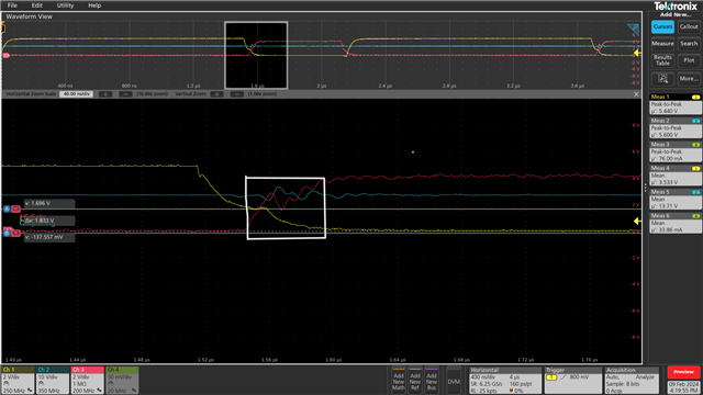
The issue is when I am observing the High-side Gate to Source voltage the Voltage is rising till a certain value (say 4V) and then again dipping to a voltage (say <2V) and from there the voltage again rises and reaches the VGS rated voltage. So I have tried to overcome this issue by adding gate resistors, snubber and also trying change the CBoot capacitor but I have not seen any difference. So I wanted to refer to the Block diagram for the knowing the proper functioning of the IC i.e., How does the IC Turns ON & Turns OFF the MOSFET exactly and if any transient is there which factors are effected in the IC and how that effects switching (ON & OFF times).


As you can see I have highlighted the Section where the DIP is occurring and the same behaviour is not observed in the Low-side MOSFET.

So just provide the explanation of the Control loop how does the switch is exactly happening including the active dead time feature.
Thanks & Regards
Mahankali Nikhilindu Kasyap
Hello Mahankali,
The device looks at the respective gate drive voltage on the falling edge, once it's at a safe level, the command to turn on the complimentary FET is given. I suspect that higher input voltages make the situation worse. I have attached an article that address this issue known as DV/DT immunity ot DV/DT shoot through. Basically, when the HS MOSFET turns on, current is injected through the CRSS of the LS MOSFET snapping it back on again.
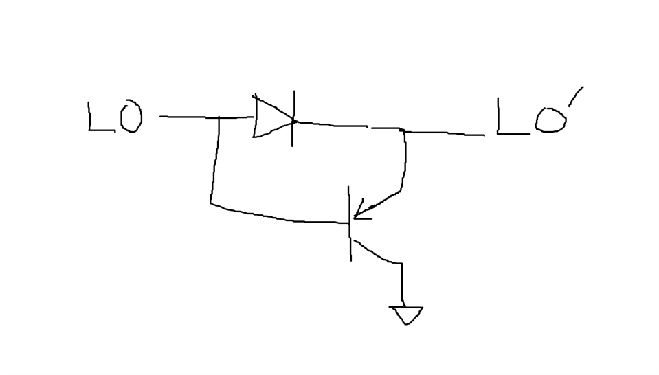
I would try a Gate resistor in the HS MOSFET first. If you cannot control this issue, please look at your layout, the gate drive traces must be routed differentially with their respective return paths, GND plane is the return on the LS FET gate. Another thing you can do is place this circuitry next to the gate of the MOSFET. This circuit uses a Schottky and a small signal pnp to clamp the voltage low.

Other things you can try is place a 10k from Gate to source of the LS MOSFET to help discharge the gate of the LS MOSFET, this may help in mild cases. Also, you could look at the QGD/QGS ratio, you would like a low QGD in comparison to the QGS. Change to a LSFET with a better ratio.
Hope this helps.
David.