This thread has been locked.

If you have a related question, please click the "Ask a related question" button in the top right corner. The newly created question will be automatically linked to this question.

UCC28C50-Q1: PSR feedback diode heating issue.

Part Number: UCC28C50-Q1
Other Parts Discussed in Thread: UCC28C56EVM-066, UCC28C50

Hey TI Team,
I hope you are doing well.
We are using TI's current-mode PWM controller IC (UCC28C50QDRQ1) for our flyback converter in our ongoing project. Below are the specifications for the flyback converter:
Flyback Converter Specifications

Flyback Converter Specifications
Sr. No. Parameter Min Typ Max Units
1 Input voltage 60 100 150 V
2 Output voltage 12.5 13 13.5 V
3 Power 30 W
4 Current 2.2 2.3 2.4 A
5 Switching Frequency 100 kHz
Transformer Specifications : 750343803
1 Np:Ns 5.5
2 Np:Na 4.14
3 Primary Inductance 75.00 uH


We've encountered the following issues and taken initial steps to address them:

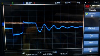
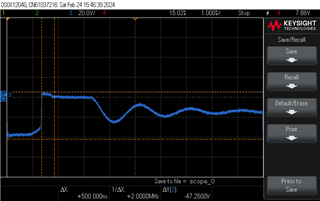
  1. Load regulation issue: The output voltage decreases significantly from 13.5V to 7V when the load varies from 0A to 2.5A. We resolved this by replacing the schottky diode with a PN diode in the PSR network at the auxiliary winding, successfully addressing the output voltage dropping issue.
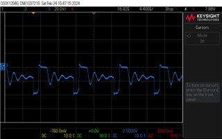
  2. Diode heating: Despite diode replacement efforts, the diode temperature reaches to 100°C, even with a 1W PN diode, raising concerns about thermal management.
  3. Output voltage instability: Despite the implementation of a zener diode at the output, the voltage continues to rise in a no-load condition, a behavior not observed with the original schottky diode. However, a 0.5W zener diode proves insufficient and overheats.

Please find attached the schematic for the design. The diodes that are causing concern have been highlighted within the schematic.
We would greatly appreciate your support and expertise in resolving these challenges.

Flyback_Maxwell-TI.pdf

  • Hi,

    1.

    Our EVM, UCC28C56EVM-066 regulation from 10% load to 100% load is about +/- 4%. Lower than 10% load, the transformer leakage starts to play big role for load efficiency. What is your input voltage when you see 13.5V to 7V? If the input voltage has effect, then your transformer turns ratios may need to adjust. But your message seems this is not an issue any more.

    2. 

    Do you mean the diode in your aux loop? You need to measure the diode voltage and current - it looks likely due to a high reverse recovery power losses. If this is true, you may need to make trade offs between the Vout regulation and the diode power losses, or use a further bigger diode.

    3.

    When less than 10% load, the zener at output is a must to keep Vout with certain range. 0.5W zener diode seems not enough. In addition to the zener, you would also need to add some more dummy load and also try to reduce your treansformer leakage.

  • Hi,

    The diodes need to be correctly selected with enough power dissipation capabilities. It looks your diodes selection not enough for the needed power dissipation. You need to measure the diodes voltage and current to decide correct diodes such as reverse recovery, and if the leakage causing too much voltage spikes on the output zener.

    These are what we know.

  • Hi Hong Huang,

    1. The output voltage dropped to 13.5V to 7V when input voltages ranged from 100V to 130V. Confirming that the transformer wasn't the issue, replacing the diode at the auxiliary loop from schottky to a normal PN diode resolved the issue. I'm still trying to grasp how changing the diode addressed the problem.

    2. The current across the diode at full load is approximately 30mA.

    3. Concerning the dummy load, I used a 100k resistor at the output, consistent with the EVM design. However, I suspect that a 100k resistor might not provide sufficient load. Could you advise on the appropriate size for the dummy load?

  • Hi,

    1.

    you need to compare the MOSFET Vgs and Vds to find out the difference at 100V and at 130V. I guess the difference is from your feedback. So also compare IC COMP voltage since the duty cycle is controlled by COMP and CS. So you need to measure CS and COMP waveform. The shortly is faster so your feedback may detect high voltage spikes from shortly than a slow diode then your feedback loop sensed a higher voltage from aux then made a lower duty.

    2.

    which diode? Also what about its switching waveform? You need to get its switching voltage and current to understand why its temperature is high which should be from its power losses.

    3.

    A proper dummy load depending a design. It looks your transformer has higher leakage. You can double the dummy load each time to see when it becomes ok. Or use a bigger wattage Zener. Or try reduce your transformer leakage spikes.

  • Hey Hong Huang,

    1. Unfortunately, we can not change the transformer's leakage inductance. Could you suggest another way to fix the heating problem?
    2. Below are images of the DSO for voltage drop across the AUX loop diode:
      1. The waveform of the voltage drop across the Aux diode when a Schottky diode is installed: https://drive.google.com/file/d/1s9J1ej7YQu49Ohpx60tbni28NayE4yxi/view?usp=drive_link 
      2. The waveform of the voltage drop across the Aux diode when a PN diode is installed: https://drive.google.com/file/d/1IzfohY9HawBmeBykgk-tva2rdiU90zcb/view?usp=drive_link
      3. Peak voltage across the PN diode and its time interval: https://drive.google.com/file/d/1lKKqkM_xOFtnS_K826VU8ud1fW-kJst3/view?usp=drive_link
      • which diode? Also what about its switching waveform? You need to get its switching voltage and current to understand why its temperature is high which should be from its power losses.

      The diode I was taking about was the AUX diode, and attached above is the switching waveform. The current is 30 mA constant; there is no difference in current.

  • Hi,

    My understanding to your need now is to find why a slower diode can make converter regulation work why not a Schottky, right? If so I think already provided my explanation as the leakage spikes go through a fast diode to charge up your AUX capacitor (AQ: CP 4.7UF 50V X7R 10% 0805 TDK) so the feedback loop sees a voltage higher then made the duty cycle adjustment based on AUX feedback so your converter Vout becomes lower and out of regulation. If you still want to use a Schottky then you need to adjust AUX capacitor value (AQ: CP 4.7UF 50V X7R 10% 0805 TDK) to let smaller voltage increase so the duty cycle is adjusted closer to the Vout need.

    By the way, I cannot open the google drive to review your waveforms - can you just send them as attachment to the E2E thread?

  • The waveform of the voltage drop across the Aux diode when a Schottky diode is installed:

    The waveform of the voltage drop across the Aux diode when a PN diode is installed:

    Peak voltage across the PN diode and its time interval:

    Sorry for the drive links. As you can see, a peak of 30 volts is seen across the AUX diode, and it heats up when a PN diode is used (the output voltage doesn't drop but the output Zener diode heats up and cannot provide output regulation when no load is attached), but when a Schottky  diode is used, there are no peaks across the diode (but the output voltage drops down). We need help with output regulation and to solve these heating issues too. 

  • Hi,

    It sounds like the output diode would have higher voltage spikes when the aux diode has lower spikes. Or the output voltage has lower spikes but the aux has higher spikes.

    Can you capture the output diode waveform to confirm this? If this is confirmed then the heat up of the output diode would be due to the higher spikes. Then a possible solution would be add snubber on the output diode to reduce its spikes. Other things can be done would make better coupling between the output winding and the input (primary) winding to reduce the leakage to help reduce the spikes.

  • Hey Hong Huang,

    I hope you're doing well. I've been encountering a few issues with our design that I could really use your expertise on. Here's a breakdown of what's been happening:

    1. Primary Side Issue: Mosfet Premature Clamping

      • I've noticed that the Mosfet's VDS is clamping at around 100V across various input voltage ranges. This is happening even though I've applied a primary side clamp of 320V, following the design of the UCC28C56EVM-066.
      • I've been using the Infineon IPBE65R050CFD7AATMA1 Mosfet, which typically has a VDS of 600V. So, it doesn't seem like the issue lies with the Mosfet itself. However, I'm uncertain if this premature clamping is causing any other issues within the design.
      • You can see the waveform for Vds below. 

    2. Auxiliary Issue: Impact of AUX Diode's Reverse Recovery Time

      • I'm keen to understand how the reverse recovery time of the AUX diode influences the overall system performance.

      • When I swapped out the original diode (Schottky:AQ: SD_200V 2A SMF) with a PN diode (S1DHE3_A/H: 1.8uS) boasting a faster reverse recovery time, I encountered a significant problem. The output couldn't deliver the expected 2.5A of current at 13V. Instead, it only managed around 1.7A at 100V input and approximately 700mA at 60V input. Surprisingly, the output voltage dropped to nearly 0V under loads >1.8A at an input voltage of 100V, but it spontaneously recovered to about ~14V when the load was removed (in no-load conditions).

        This experience was quite different from what I observed when using a diode with a slower reverse recovery time (BYG10YHE3: 4uS) at AUX loop. With this diode, I noticed current outputs ranging from 1.6A at 60V input to 2.7A at 130V input. However, drawing additional current beyond this threshold caused the output voltage to plummet to nearly 0V. Similar to the faster diode, the output voltage recovered without needing to power cycle the device upon load removal.

      • Additionally, I'll provide a comparison of the observed peak differences between these two diodes. It's worth noting that the heating issue persisted throughout these experiments, regardless of which diode was used.

    3. Secondary Side Issue: Zener Diode Overheating
      • The 13V zener diode installed at the output experiences significant heating when a load of 0.5A is applied, particularly as the output voltage approaches around 14.5V. This excessive heating leads to gradual degradation, impacting the diode's regulation capability, especially in scenarios with no load.

      • Despite attempting to mitigate the issue by replacing the 100k resistor with a 10k resistor at the output to serve as a dummy load, the zener diode continues to heat up even under minimal loads. Interestingly, when current is drawn from the secondary, the output voltage decreases to 13V, causing the zener diode to cease regulating and subsequently cool down.

      • One potential solution I've considered is utilizing a 3W zener diode, which offers better heat dissipation. However, if the output voltage regulation remains inadequate, even the 3W zener diode heats up and maintains an output voltage of approximately 14.5V.

    • Waveforms: 

      • Channel 1- Secondary coil
      • Channel 2 - VDS
      • Channel 3 - Voltage across Aux diode 
      • Channel 4 - OUT pin of UCC28C50.
         
      1. You can see the waveform for Vds below.

    • Additionally, I'll provide a comparison of the observed peak differences between these two diodes. It's worth noting that the heating issue persisted throughout these experiments, regardless of which diode was used.

    Diode with faster reverse recovery = 1.8 uS


    • Diode with faster reverse recovery - 4uS
             
  • Hi,

    1. If the voltage Vds not high enough then 320 V TVS will not turn on. You need to calculate the reflected voltage Vr to find how much Vds can be. The Vds spikes are from your transformer leakages, your input voltage and your primary side current at the MOSFET turn off, and the reflected voltage Vr.

    I see your Np/Ns = 5.5, so when Vout = 14.5V, assume the secondary side diode voltage drop = 0.7V, your transformer reflected voltage Vr = (14.5V + 0.7V) x 5.5 = 83.6 V. It looks this is the reason why you see about 100V Vds.

    As your reflected voltage is at about 100V, then 320V TVS looks not good to your design which may demand your MOSFET with higher Vds rating but in reality not needed. You may consider to use 160V TVS for the clamp.

    2. The Vout is based on FB voltage. You can measure FB pin voltage to compare different diode on Aux effect. To achieve good Vout regulation our experience is using slower speed diode so the leakage spikes have less effect on the FB than a faster diode but also need the capacitor value tune up to help Vout regulation.  So only capture the waveform on the aux diode is not able to tell why - the key is how FB pin voltage is obtained which relies on the aux diode, the transformer leakage, the coupling from Vout to AUX, the capacitor value (AQ: CP 4.7UF 50V X7R 10% 0805 TDK). You need tune up these to get best the Vout regulation range. Note, for the AUX regulated Vout, Vout can only achieve good regulation in a load and Vin range due to the leakage and coupling limitation.

    3: If your transformer has higher leakage spikes over the zener voltage the secondary side Zener is turned on more so it’s heated up more. So if you cannot make the spikes less you would have to use bigger wattage Zener or change Zener voltage to be higher.