Hello all,
We are using TPS62842DGRR as buck converter for two CR123 batteries connected as series and resulting about 6.2V as DC-DC supply. During HW test of our devices we found that some devices have failed 3.3V DC power load test. After some investigation we observed that IC with marking 34J makes huge waveform noise on power rail (200mV peak to peak) during adding loading 7.4 Ohm. Also additionally it's making hearable noise sound.
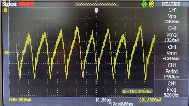
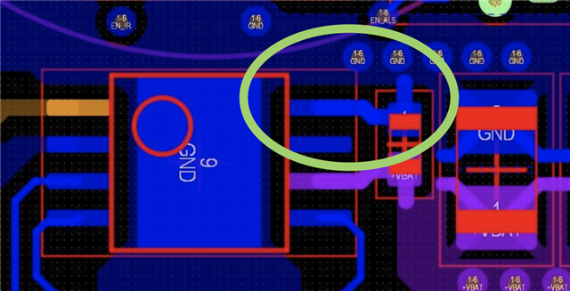
The main reason is that our devices utilises about 220 uF as a total capacitance for 3.3V power rail during enabling different power domains, also PCB layout is sightly different than it’s on data sheet recommendation (See attached image), especially GND pad #8 (In green circle). The primary observation that components with marking 24J or 16J operates without any noise injection. Also when we made a short connection of GND pin #8 to GND polygon pour directly without the trace on component with 34J marking, the noise became as usual and device passes the test. We already made a fixes to PCB, but we have a lot of already produced PCBs which we would like to use for production:
We would like to know the importance of this problem and why 16J and 24J are working fine but 34J and 35J aren't? What is different? And decide the final way to solve it for already produced PCB. As we see there are couple ways to solve it:
- Finding the components with 16J or 24J marking;
- Reducing the overall capacitance of 3.3V rail;
- Applying the manual fix (making the short connection of pin 8 to nearby GND polygon.