A related question is a question created from another question. When the related question is created, it will be automatically linked to the original question.
If you have a related question, please click the "Ask a related question" button in the top right corner. The newly created question will be automatically linked to this question.
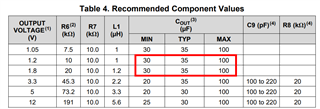
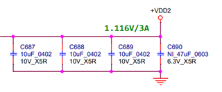
1. We have a recommended LC table which lists recommended effective Cout, as shown below. Have you checked your effective Cout? I'm worried your capacitance may be not enough.
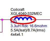
2. For safety use, we suggest to select the inductor with Isat higher than device current limit. Because in some cases (e.g. output short to ground), current limit could be triggered and we don't want inductor to be saturated. Below inductor Isat is quite small.
For layout,
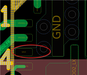
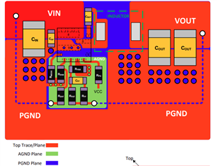
1. We don't suggest AGND connected to PGND directly under IC, because PGND is noisy here. Please put the connection to a farther quiet place.
2. Suggest to connect Rfb/Rmode/Ren ground to AGND, not PGND, see datasheet layout example.
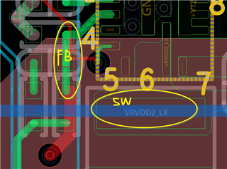
3. Sensitive FB trace is quite close to noisy SW node, which is not good. Please place the FB trace farther away.
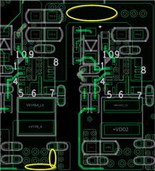
4. Have you checked each via max current? If your actual loading is large, you may place more vias for Vin/Vout polygon.