This thread has been locked.

If you have a related question, please click the "Ask a related question" button in the top right corner. The newly created question will be automatically linked to this question.

LP8764-Q1: LP8764-Q1 Circuit design questions

Part Number: LP8764-Q1

hello
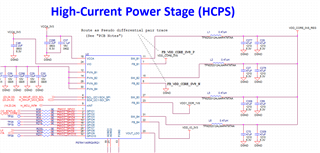
I have a question about the P876411A5RQKRQ1 used for the J721S2 PDN.
I am trying to tie Buck 1,2,3,4 together and use them as High-Current.
Is the voltage fixed at 0.8V? Or do I need to program it?

I understand that P876411A5RQKRQ1 FB1~2 is connected to VDD_CORE_0V8_REG in J721S2 EVB schematic.
I don't understand why FB3 is connected to VDD1_DDR_1V8 and FB4 is connected to VDD_IO_3V3.
Is there any reason?

Also, I don't want to use GPIOs, but leave the pin floating?

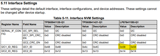
Also, I need to know the slave address to use I2C, but I don't see anything in the datasheet to set the slave address.

  • Hi Jae,

    First of all, the device P876411A5RQKRQ1 is very old. But can be used for certain R&D purpose with updating NVM. Since this device has been originally defined to be used together with TPS65941120-Q1 and TPS65941421-Q1 the LP876411A5-Q1 cannot work alone without reconfiguring device. Devices interconnection bus expects devices to be connected together.

    By creating new NVM config voltage can be permanently changed to another level. 

    If you don't want to use GPIOs how you want voltage startup/shutdown to be controlled?

    For I2C address please see:

    https://www.ti.com/lit/ug/slvucj9/slvucj9.pdf 

    BR, Jari