This thread has been locked.

If you have a related question, please click the "Ask a related question" button in the top right corner. The newly created question will be automatically linked to this question.

TPSI2072-Q1: Designing with TPSI2072

Part Number: TPSI2072-Q1

Hello Team,
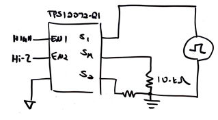
We are planning to use the device TPSI2072 for one of our applications.
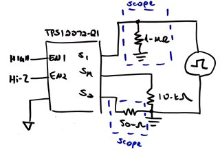
The device is used for muxing some 12V signals.
The input will be connected to the SM pin of the device and S1 will be connected to one device and S2 will be connected to another device.
EN1 and EN2 will be used to select the signal flow.
When EN1 is high and EN2 is low, the signal will flow from the SM pin to the S1 pin and to the end device.
similarly for EN2.
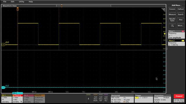
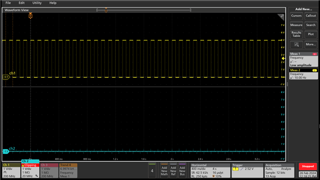
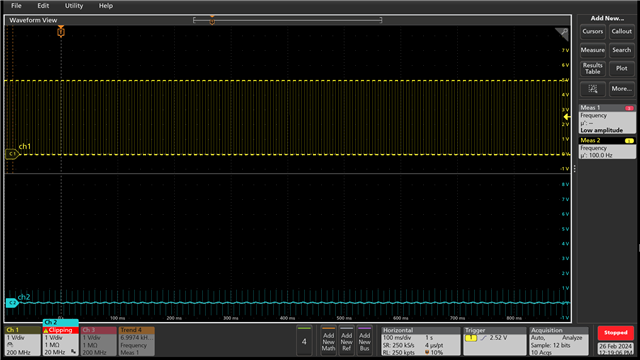
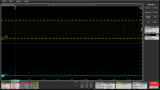
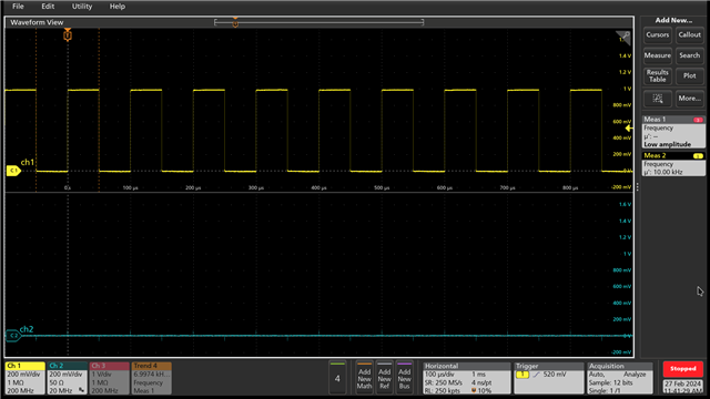
When high frequency signal is fed at the SM pin, is there any possibility the signal could be present at the S2 pin even if only the EN1 is selected (due to the parasitic capacitance of the MOSFET)?


Looking for your reply.

  • Hello Sv,

    Thanks for checking with our team on E2E. Can you share more details about your application (e.g. frequency, digital/comms) and is isolation needed here? Our part was not designed with high frequency in mind, you may consider a device from the multiplexer portfolio instead. 

    Best regards,
    Tilden Chen


    Solid State Relays | Applications Engineer

  • Hello Tilden,
    Thank you for your reply.
    This is not a high frequency application.
    The S1 and S2 pins will be some ADC pins.

    Our part was not designed with high frequency in mind

    I was curious about the channel to channel cross talk due to parasitic capacitance

  • Hello Sv,

    Thanks for the update. I am checking with my team about the crosstalk frequency between the two secondary channels and will get back to you here.

    Best regards,
    Tilden Chen


    Solid State Relays | Applications Engineer

  • Hello Sv,

    Thanks for your patience. I took a look at your question in the lab today and monitored the voltage on (single-ended probes, built-in 8-pF capacitance) at S2 while applying a square wave to S1-SM (S1-SM on, SM-S2 off) and stepped up the frequency by decades. This is what I saw. I imagine adding some input capacitance in the nF range at the ADC pins would filter out the spikes. Can take a further look if you are interested but wasn't sure what frequency range you were expecting and the speed needed at the ADCs. 

    Setup

    1-Hz

    10-Hz

    100-Hz

    1000-Hz

    Best regards,
    Tilden Chen


    Solid State Relays | Applications Engineer

  • Hello Sv,

    Another update here, I tried changing the setup some more. I think the parasitic capacitance sends a certain amount of current through so using a larger termination resistance would result in a higher voltage reading and appear less flattering. I adjusted my setup to use a 50-Ω termination on S2 and saw the following measurements at 1-Hz to 100-kHz. 

    Setup

    1-Hz

    10-Hz

    100-Hz

    1-kHz

    10-kHz

    100-kHz

    Best regards,
    Tilden Chen


    Solid State Relays | Applications Engineer