This thread has been locked.

If you have a related question, please click the "Ask a related question" button in the top right corner. The newly created question will be automatically linked to this question.

CSD18542KTT: Designing with CSD18542

Part Number: CSD18542KTT
Other Parts Discussed in Thread: CSD18540Q5B, CSD19505KTT, LM9061-Q1

Hello Team,A.

We want to select an N channel based on the following specifications.


90A continuous current
200A pulse (100uS)
150A pulse (1mS)
Low RDSon
Low input and output capacitance
The MOSFET is used to turn on/off the power to a board (48V system).

Can I use the MOSFET CSD18542KTT for our application?


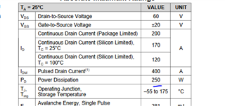
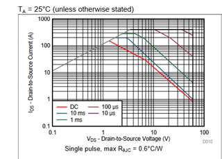
How is the VDS related in SOA.
The above graph shows a DC drain current of more than 120A when VDS is above 1V.
The VDS is the product of RDS and te drain current
The RDS of the device is 3.3-mΩ and the ID is 90A.
So the VDS will be only 297mV.
Please correct me is I am wrong.

Can anyone check whether the device is working in SOA or not?


Looking for your reply

  • Hello Sv,

    Thanks for your interest in TI FETs. Please see blog at the link below for more information on on how TI tests and specs SOA for our FETs. The straight line that goes from the vertical axis up to the right is known the Rds(on) limitation is a constant on resistance of the device.A 60V FET such as the CSD18542KTT might work for your application but you need to know the maximum input voltage range and how much margin is required on the breakdown voltage of the FET. Some customers opt for 80V or 100V FET for 48V input depending on their particular requirements.

    For 90A continuous current, you will probably need to parallel 3 to 4 devices to reduce the conduction loss and spread the heat across several packages. If you're OK with a 60V FET, then with 3 x CSD18542KTT in parallel, each FET will dissipate about 4.7W which is pushing the capability of the package (4W max). With 4 x CSD18542KTT in parallel, the conduction loss per FET is reduced to about 2.7W per FET which is within the capabilities of the package. You might also want to consider the CSD1850Q5B 60V FET in 5x6mm SON package. It has lower Rds(on) and is smaller package. With 3 x CSD18540Q5B in parallel, the conduction loss per FET is about 2.5W Which is within the capability of this package (3W max). If you want a higher voltage FET, then I would recommend the CSD19505KTT, 80V FET in D2PAK.

    How are you driving the gate of the FET? Are you using a hot swap controller? SOA is of concern when the FET is operating in the saturation region (Vds > Vgs - Vth) where there is voltage across the FET while current is flowing thru it. For the 100µs and 1ms pulses, is the FET fully turned on or do these occur during turn-on of 48V to the board such as an inrush event? Are they single pulses or repetitive/periodic? The second link below is to an application brief on using the SOA graph in a design. Please review and let me know what else I can do to to help.

    http://e2e.ti.com/blogs_/b/powerhouse/archive/2015/05/02/understanding-mosfet-data-sheets-part-2-safe-operating-area-soa-graph

    https://www.ti.com/lit/pdf/SLUAAO2

    Best Regards,

    John Wallace

    TI FET Applications

  • Hi Sv,

    Following up to see if your issue has been resolved. Please let me know.

    Thanks,

    John

  • Hello John,
    Thank you for your reply.
    Sorry for replying late.
    The system is 24V system and I hope it is okay to use a 60V MOSFET.
    Please correct me if I am wrong.
    Also, we are using the Gate driver LM9061-Q1 for driving the MOSFET.
    So the maximum Gate Source voltage will be 15V.
    Can you please explain how the 4W max for the MOSFET CSD18542KTT  is calculated.
    The datasheet says 250W.

    and the I^R gives only (90*90*5.1mΩ) = 41.31W.

    The continuous current of the device CSD18542KTT is 120A.

    So why cant we use a single MOSFET for 90A applications?.

    SOA is of concern when the FET is operating in the saturation region (Vds > Vgs - Vth)

    In our application VGS is 15V.
    Vth ( I hope it is VGSth) is 2.2V max.
    VDS is ID*RDS (Please correct me if I am wrong) is 90*5.1=0.459V.
    So the MOSFET is working in saturation mode.

    Also, while looking into the graph,


    At low VDS, the current seems to be low only about 10A.
    Actually at this time, the power drop across the MOSFET (VDS*IDS) will be very less (more safe for the MOSFET)
    While if the VDS is increased to above 1V, the current will be above 100A, very high voltage drop across the MOSFET.
    Why this is so?.
    How we can increase the VDS of a MOSFET to carry more current?
    While operating MOSFET as a switch, we need a low voltage drop across the MOSFET.
    Please correct me if I am wrong.

    I know some of my understandings about the MOSFET are wrong.
    Please correct me.

    Looking for your reply.

  • SV,

    John is out until Tuesday , I will try to answer some of your questions:

    1. Regarding MOSFET current ratings
      1. Essentially these are calculated for silicon limit based off an ideal set of conditions. See the link here https://www.ti.com/lit/an/slvafg3c/slvafg3c.pdf  for all our technical MOSFET content, section 1 understanding MOSFET datasheets, there is a section on continuous current ratings explained. As such the maximum power dissipation is very large in all MOSFET datasheets, this is the industry std for all MOSFET vendors.
    2. KTT 4W limit question
      1. In the link https://www.ti.com/lit/an/slvafg3c/slvafg3c.pdf in section 4 there is an article called "selecting the right power MOSFET/power block for your application", this explains where the 4W comes from. This 4W is not a maximum capability of the device but simply what we see as the typical capability of a package on a typical application board vs the idealized calculated value of power dissipation which is never realistic as everything needs to be kept to 25degC etc.
    3. SOA question of Rds(on) limit line -  "At low VDS, the current seems to be low only about 10A"
      1. The Rds(on) limit line in the SOA for all MOSFETs from all vendors is a linear dependency between Vds and Ids. The line slope is he  max resistance of the FET @ max junction temperature. So points on the line are given by the equation Ids = Vds/Rds(max). Device is fully enhanced and slope/points are simply a calculation assuming Tjmax not exceeded

    I hope this helps answer your questions

     Many thanks for your interest in our devices

    Regards

    Chris Bull