This thread has been locked.

If you have a related question, please click the "Ask a related question" button in the top right corner. The newly created question will be automatically linked to this question.

LM5177: Request to review LM5177 schematic.

Part Number: LM5177


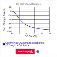
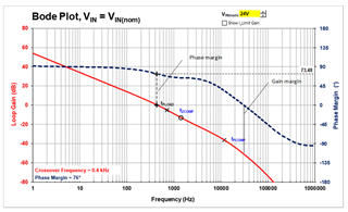
Please review the LM5177 schematic. If there are any errors, please guide me.

In some cases my system can be supplied with a Vin of 12V, 24V or 48V and all three will work fine.
Power comsumption is Max 60W and typ 45W.

LM5177_REVIEW.pdf

  • Hi lee,

    Thanks for using the e2e forum.
    Could you please fill in our quickstart calculation tool for LM5177 and send it back to us?
    This will speed up the review process.
    https://www.ti.com/tool/download/SNVR519

    Thanks and best regards,
    Niklas

  • Hi, Niklas Schwarz 

    New schematic and calculation tool is here , Please review and guide me. 

    8371.LM5177_REVIEW.pdf7723.LM5177 Buck-Boost Quickstart Tool V1_0_9.xlsm

    thanks 

  • Hi lee,

    Thanks for filling in the tool.
    We will review the design and get back to you within 1-2 days.

    Thanks you very much for your patience.

    Best regards,
    Niklas

  • Hi, Niklas

    Please respond to review.

    thanks.

  • Hi Lee,

    please see my comments below

    • Sense resistor is to low - only 10% margin and still higher then suggested
    • Losses are very high - please check again if this can be handled
    • Ensure input caps are added - not shown in schematic
    • Check filter for Rcs - change 100 to 10 Ohm
    • Snubber on SW1 and SW2
      Place Footprint for a snubber at SW1 and SW2
       (they can then be populated in case needed (e.g. due to EMI) without layout change)
      Note: Snubber: connect Resistor to GND for better Thermal performance
    • Add Series Resistor into MOSFET Gate signals lines
      (they can then be replaced in case needed (e.g. due to EMI) without layout change,
      additional option: add a diode in parallel for slow on and fast off.
    • Remove Cap on MOSFET Gate - already marked as DNI - so should be OK
    • If needed increase pull low resistor on MOSFET gate to at least 100k
    • Remove L138, L137

    • Cap at VCC 47uF : (Datasheet min: 10uF with DC Bias
      please check the cap on Vcc to have the required capacitance considering DC BIAS - we use a 47uF on the EVM
    • Miller Plateau of MOSFETs to high
      used MOSFETs need to be logic level MOSFETs - can be seen by Miller Plateau in the range of 2.5V-3.5V
    • R879 do not add !
    • Cross over Frequency could be increased

    Best regards,

     Stefan

  • Thank you for Reply. 

    1. Sense resistor is to low - only 10% margin and still higher then suggested
    -> Are you saying to change it to 1.9mm ohm?

    2. Losses are very high - please check again if this can be handled
    -> Changing the inductor value to 3.3uH improves efficiency. However, it turns into a red square. Is there a problem if I increase the inductor value?
    -> How can I increase efficiency?

    3. Ensure input caps are added - not shown in schematic
    -> Added 100uF.

    4. Check filter for Rcs - change 100 to 10 Ohm
    -> Changed R868 and R873 to 10 ohm.

    5. Snubber on SW1 and SW2
    Place Footprint for a snubber at SW1 and SW2
    (they can then be populated in case needed (e.g. due to EMI) without layout change)
    Note: Snubber: connect Resistor to GND for better Thermal performance
    -> Snubber circuit added to Q75 and Q76.

    6. Add Series Resistor into MOSFET Gate signals lines
    (they can then be replaced in case needed (e.g. due to EMI) without layout change,
    additional option: add a diode in parallel for slow on and fast off.
    -> There is already a resistor at the gate, a diode was added to the FET.

    7. Remove Cap on MOSFET Gate - already marked as DNI - so should be OK
    -> ok

    8. If needed increase pull low resistor on MOSFET gate to at least 100k
    ->Added 100k ohm

    9. Remove L138, L137
    -> -> Why is it not connecting?? Does it work even if I remove L137?

    10. Cap at VCC 47uF : (Datasheet min: 10uF with DC Bias
    please check the cap on Vcc to have the required capacitance considering DC BIAS - we use a 47uF on the EVM
    -> No modification.

    11. Miller Plateau of MOSFETs to high
    used MOSFETs need to be logic level MOSFETs - can be seen by Miller Plateau in the range of 2.5V-3.5V
    -> Is there a FET you can recommend? Please Recormend FET.

    12. R879 do not add!
    -> R879 DNI

    13. Cross over Frequency could be increased
    -> What should I do? Please tell me how to solve it.

    Please respond to any additional questions. I would like to apply your review to create a perfect circuit.

  • Hi Lee,

    The issue is that you have a very large input voltage range which makes it hard to optimize.
    Do you need the full output power (6A) over the full input range?

    You are right with the current configuration you can not increase the inductor otherwise you will not get the required current signal.
    So you may need to check if the used inductor can handle this losses or need to add additional cooling.

    9. L138, L137 is shown as inductor - the connection is needed but not the inductor

    10. What is the effective capacitance of the used capacitor at VCC with 5V supply?

    11. Selecting a MOSFET is a quite time consuming process with checking the performance and losses in the application over the full range and with deciding what parameter are most important. The Excel calculator can help you here.
    When selecting the MOSFET please ensure that the Miller Plateau is below ~ 3.5V - for the BSC037N08NS5 you can see this in Diagram 14 of the datasheet.

    13. the Excel calculator can help you here as well: Set the desired Cross over Frequency to a higher Value e.g. 5kHz and then use the suggested compensation values. Check the Bode diagram in the full operation range: 

    • Phase Margin should be greater 60 Degree.
    • Transition of Gain at 0 dB should be with -20dB/Decade,
    • Gain margin should be < - 12dB

    Best regards,

     Stefan

  • Our customer wants to use all 12V, 24V, and 48V systems.
    Ultimately, Our Development Board must operate on three voltages.

    Isn't LM5177 a suitable solution in this case? Are there any other solutions?
    It varies depending on the load, but the maximum power consumption is 60W (10V, 6A).

    9. ->Yes, uderstood

    10. -> How can I calculate effective capacitance? Can I just use the 47uF used in the EVM?

    11. -> What problems will occur if I use SQJ422EP-T1-GE3 used in EVM?
    I'm looking for Vds=Min 60V in case Vin=48V. Did I understand this correctly?

    13. -> How high should I raise the crossover frequency?

    Phase Margin should be greater 60 Degree. -> This can be checked in excel.
    Transition of Gain at 0 dB should be with -20dB/Decade, -> Can I check it in excel? How can I check this?
    Gain margin should be < - 12dB -> Can I check it in excel? How can I check this?

    thank you 

  • Hi Lee,

    the LM5177 can be the right device - maybe the design spec needs to be more clear.

    The 3 voltage above are the input voltage ?

    If yes, why are the input range in the Calcualtor set to 4 - 60 V?

    10. this you will find in the capacitor datasheet e.g.  this cap has at 5V only 20% of the 22uF

    11. just enter the parameters of the MOSFET and check if the losses are OK for you

    13. this can be done by adopting the compensation section of the quick start calculator see : Desired Crossover Frequency
    - the bode plot shows you then the result, here you also seen and can check the 3 criteria discussed above

    Note: More info on compensation can be found in this great report: Switch-mode power converter compensatin made easy

    Best regards,

     Stefan

  • Hi Stefan,

    Thank you for your kind reply.

    The three voltages are input voltages.
    The reason Vin is specified as 4V~60V is because of the test in the attached document.

    test1.docx
    What should I do to optimize LM5177?

    10 -> uderstood ,
    I checked the capacitor used and it was only 5uF. I'will need to change capacitor.

    11 -> Yes.

    13-> Phase Margin can be checked in Excel calculator. However, Transition of Gain at 0 dB and Gain margin were not found.
    How can I check this in Excel calculator?

    thank you

  • Hi Lee,

    OK, this is for cold crank - so the duration is only for a shorter time - this can relax the thermal issue.

    For the gain and phase margin see the image below

    Note: More info on compensation can be found in this great report: Switch-mode power converter compensatin made easy

    Best regards,

     Stefan

  • Hi Stefan,

    The switching frequency was reduced and the output voltage increased from 10V to 16V.
    So I was able to increase the inductor to 3.3uF without any red space. We also used the same MOSFETs used in the EVM.
    More efficiency and less loss than ever before. Please review.

    LM5177 Buck-Boost Quickstart Tool V1_0_9-2nd-16V.xlsm

    1055.loss_compare.pdf

  • Hi Lee,

    looks OK from my side

    Recommend to properly test the cold crank are for the heating of the components on the real hardware to see how the temperature increase behave.

    Best regards,

     Stefan