This thread has been locked.

If you have a related question, please click the "Ask a related question" button in the top right corner. The newly created question will be automatically linked to this question.

LM5113: Highside switch timing topic

Part Number: LM5113

Hi,

in designing a Class-D audio amplifier I encounter a topic which I do not understand.

The circuit depicted below has been simplified for debugging reasons. The input signals for the LM5113 (PWM_LEFT_Delay and PWM_INV_LEFT_Delay) are 50% duty cycle 5V signals with a frequency of 500kHz. In order to prevent a cross current in a half bridge, they have a dead time of 20ns.

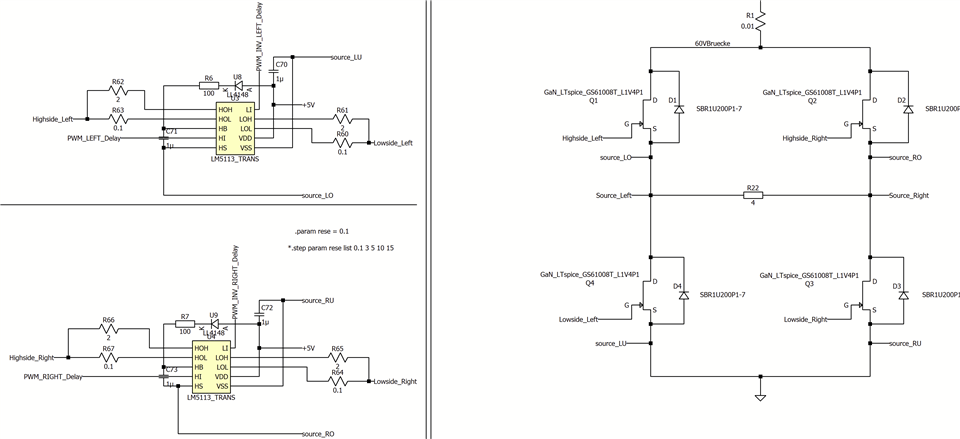
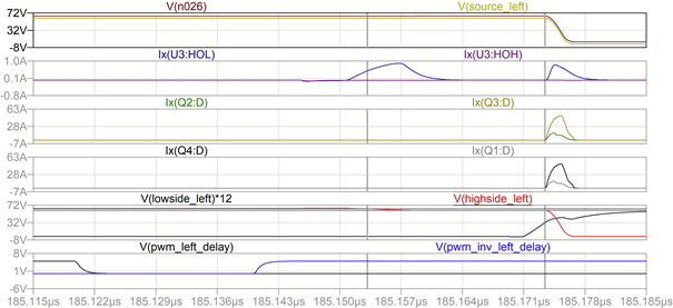
In the simulation however there is not really a dead time when the gate signal of a high side switch (Highside_Left) falls. For approximately 20ns, Highside_Left will fall by only 4.8V (the value, the gate signal is above supply voltage during boost). Only when the time comes that the gate signal of the low side switch (Lowside_Left) rises, Highside_Left will finally fall to zero. It can be seen, that the HOL pin of the LM5113 delivers current in two phases: first, when Highside_Left falls by 4.8V and then once again when it falls to zero. Obviously HOL is floating during the 20ns in between. As a consequence a cross current is flowing beween the high side switch and the low side switch (despite of the dead time in the LM5113 activation signals).

Could you help me to understand and fix this topic?

Best regards

Helmut

  • Hey Helmut,

    Thank you for your question regarding the LM5113.

    What is the right side of the system doing while this is occurring? Are they the same as the left side or equal but opposite or completely different?

    Why are you connecting the switch nodes with the 4 ohm resistor (R22)?

    Do you have a load connected to the system? If not, the switch node will be left floating and improper switching will occur.

    For your bootstrapping circuit, the 100ohm resistor is too large. In Section 7.3.2 of the datasheet, it is recommended to use a 20ohm series resistor and either a BAT46, BAT41, or LL4148 bootstrap diode. Also, the bootstrap capacitor sizing is outlined in Section 8.2.2.2 with the VDD bypass capacitor sizing outlined in Section 8.2.2.1. Using these guidelines, you should have approximately 100nF capacitors here.

    Let me know your responses to these questions and if you have any further questions.

    Thank you,

    William Moore

  • Hey Helmut,

    Are you measuring HO with reference to ground or HS? If you are measuring with respect to ground, HO not be low (0V) until HS goes to ground because when HI is low, HO-HS is 0V but HS is not 0V until LO goes high. So, for measuring HO, you need to measure with respect to HS.

    Let me know if you have any other questions.

    Thank you,

    William Moore

  • Hey William,

    thank you so much for your fast response.

    the Class-D amplifier uses a 3-level (or 3-point) PWM. Unlike in a 2-level PWM, both high side switches (MOSFETs) or both low side switches may be activated simultaneously. This happens when the input signal is zero and the latter is valid in my simplified xsection. (A 3-level PWM produces less ripple compared to a 2-level PWM.) So, in the situation which I presented the right side is doing the same thing as the left side. However I am observing the same problem with an input signal unequal zero.

    The four ohm resistor represents the load (a loudspeaker). Originally there is a filter between the bridge and the load but I have taken it away from the xsection in order to simplify it (same problem when the filter is in, but the filter complicates the analysis due to its inductive currents). The four ohm resistor is the load.

    I appologize for my schematic because originally I had used a 100nF capacitor. I tried a 1uF capacitor as I wanted to try out whether there is a change in the behaviour, but the problem is still there. So, originally I am using a 100nF capacitor.

    Could it be, that the data sheet has changed over time? In my version in section 7.3.2 it says: "The LM5113-Q1 requires an external bootstrap diode with a 100 Ω series resistor from VDD to HB to charge the
    high side supply on a cycle by cycle basis. The recommended bootstrap diode options are BAT46, BAT41, or
    LL4148." In the meantime I have parameterised the resistor and tried out 20Ohm and 100Ohm but the behavior is still the same.

    Anyway, your answer has helped me a lot and especially the next message you sent, helped me to understand my topic. Thank you very much once again!

    Best regards

    Helmut