This thread has been locked.

If you have a related question, please click the "Ask a related question" button in the top right corner. The newly created question will be automatically linked to this question.

CSD87381P: CSD87381P layout review and check

Part Number: CSD87381P

Dear Guys:

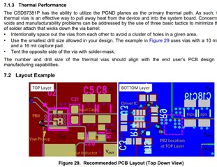
         For CSD87381P, there are 9 through holes in the pink frame, 2 of which are on PGND and the other 7 are around PGND, right? If we have a VIA with layer1 to layer2 (GND), can we do this without drilling a through hole? We must do you want to fight so much?
Tommy

  • Hello Tommy,

    Thanks for the inquiry. I believe all of the vias under the part within the pink rectangle and the other two vias outside it are connected to PGND. The idea is to maximize the PGND copper under and around the device on the side of the PCB onto which it is mounted. The thermal vias take the heat from the part, distribute it into the PCB and then to ambient. TI used thru-hole vias on the application board (shown in the recommended layout example) for testing the device in a synchronous buck converter. We have not done any testing with blind and buried vias which just go from layer 1 to layer 2. I think it should be OK if layer 2 is a GND plane but the effective thermal resistance may be higher because the thru-holes provide a path to ambient on the backside of the PCB. I would be more than happy to review your schematic and PCB layout. You can contact your TI FAE or email me directly at jwallaceri@ti.com.

    Best Regards,

    John Wallace

    TI FET Applications

  • Dear John:

             I have sent the schematic and layout to you by your TI mail (jwallaceri@ti.com).

    Tommy

  • Hi Tommy,

    We will review and provide our feedback.

    Best Regards,

    John

  • HI Tommy,

    Since we have moved this discussion to regular email, I am going to close this thread. Please email me if you need additional assistance.

    Thanks,

    John