This thread has been locked.

If you have a related question, please click the "Ask a related question" button in the top right corner. The newly created question will be automatically linked to this question.

TPS65987D: TIDA-050014 Based Production Tester Support

Part Number: TPS65987D
Other Parts Discussed in Thread: TPS65988, , TIDA-050014, TPS65987, TPD4S311A, TPD6S300A

Dear TI,

Supporting a large production run consuming a lot of TPS65988 we designed a production test fixture that leverages the TIDA-050014 reference design to negotiate 9 and 15V profiles from our TPS65988 based device under test.  The block diagram attached shows a simplified concept where the processor on the DUT is using a port expander to 'press' the 5V, 9V and 15V buttons on the TI Sink board (TIDA-050014) and overall this concept works pretty well.  Recently we've had a failure in the test board that's require replacement of the TPS65987D chip and a few weeks later that circuit failed again.  It happens to be sink #16 on the test board.  We're updating the test board now to correct a few issues and we've recalled the test board with the failed TPS65987D to investigate.  The board arrives tomorrow AM and I'm going to connect the Aardvark and try to debug the damaged circuit.  I'm looking for any input you have as to what I can test to determine root cause and I will send you additional information after I have the board in hand and can probe it for physical defects.

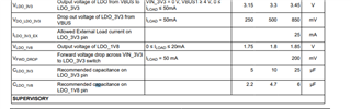
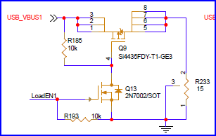
The timing of the test is not overly fast - we allow a few seconds at each voltage and we also connect a small load (a 15 ohm resistor) during test.  Both ends should support 3A, and at most we're puling 1A during test.  The snip pasted below shows 1 of the sixteen test channels, followed by the majority share of the load circuit which is quite simple and also controlled by a port expander.  TI already has an old copy of our product schematic but I can provide that to you offline if you would like, just ask and provide me your email address.  I can also provide the full schematic for the test board if that's helpful.

I'm hoping that in response to this you can offer some specific registers to check, specific tests I can perform, or direct guidance on what to pull form the Application Customization Tool.  Once i have the board I plan on pulling a full debug snapshot and will provide that in addition to any other failure indications I find during visual or electrical inspection.  Those should be loaded here tomorrow - and I would also highlight any requested info you may want to see.

Thanks!

Adam

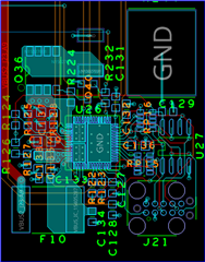
TPS65987D: Single channel sink circuit.  There are sixteen in total.

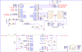
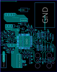
Port expanders used to press TIDA 050014 buttons and read back the feedback LED states

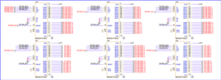
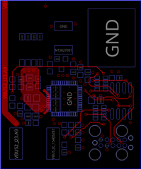
Single circuit's load.  15 ohm power resistor with body tied to ground.

Attached (simplified) block diagram:

ProductionTester-ChargingTestBlockDiagram.pdf

  • Hi Adam,

    What does sink port #16 test? Does it test something different than the other 15 ports?

    From what you shared so far, it is hard to suggest anything specific to test. It would help to know the device behavior when the TPS65987 gets damaged.

    Thanks and Regards,

    Chris

  • Hi Chris.  So the test is pretty simple.  It acts just like the eval board.  On power up, we see the 5V contract by way of the 5V LED being lit by the TPS65987D.  We press the button to negotiate 9V and test the LED output to confirm the contract is present.  We apply a load resistor as shown and validate that the right current flows.  We disconnect the load and then press the 15V button.  We connect the load and test the current again.  We remove the load, then press the 5V button (HRESET as in your reference design) and verify the 5V LED returns.  I don't recall if we apply the 5V load at this point or in the beginning, but that seems relatively moot.

    On Failure none of these functions work.  The circuit does nothing.  Replacing the chip returns normal function.  Something has failed under these simple circumstances, I'm just not sure what yet.  Like I said - the board is coming in tomorrow so that I can take a closer look as to why the device doesn't light the 5V LED or respond to the 9 or 15V button presses.  If the core responds to the Aardvark i plan on pulling a full debug snapshot.  

    All sixteen channels are identical and the test is the same for them all.  It is the most simple implementation of the eval board circuit and verifies the assembly at a very basic level.

    Is there any reason why the hardware presented shouldn't be robust?  Have you reviewed the circuit shown?

    Thanks,

    Adam

  • Good Morning Chris,

    Unfortunately we found the device is damaged such that LDO_3v3 and LDO_1V8 are shorted to ground.  They're roughly 4 and 14 ohms to ground respectively.  Digital analysis not being an option I guess we're stuck looking at the circuit and board.  

    What ideas do you have?  I am going to look to increase copper heatsinking as much as possible.  Maybe we will switch from 1oz copper to 2oz.  Here's a snip of the board and pertinent heat sinking as is which i believe may be insufficient, even though we only support 1A.   Please also review the schematic and let me know what you think.

    I would like to send you native files but not on the forum.  Please shoot me your direct email and I'll be happy to send you more.  

    Would sticking an aluminum heat sink on top of the TPS65987D offer much dissipation on this part?  

    A last thought is to pull the load resistor far away form the TPS65987D.  That's easy to do too.

    The above comments aside - which we will go ahead and do - What schematic suggestions do you have if any?

    General view:

    Top layer etch.  Move the sense resistor and get is more heat sinking vias.

    bottom layer etch: add copper pours for TPS65987D mosfet drains and ground pad.  Move from 4 layers to 6 so that the bottom traces can be moved away from heatsinking areas.

    Adam

  • Hi Adam,

    Please give me some time to look over the data you have provided. I have not done an extensive review of your schematic, but nothing stood out from a quick glance through.

    I'm surprised the LDO's are shorting to ground, they should not have significant current flowing through them. What do you have pulling load off of LDO3V3, could you get a max current/power estimate for both LDOs? Maybe you are overloading the LDOs.

    Are you seeing the PD controller heat up? From the test procedure you described, as long as you are not dumping large amounts of current through the load >5-A, I would not expect to see too many problems. For how long is the device maintaining load and how much trace width and copper do you have for the high power traces?

    Thanks and Regards,

    Chris

  • Hi Chris,

    We're not pulling anything off the 1.8V LDO.  The 3.3V LDO is only being used for the memory, W25X05CLSNIG, which draws 15mA or less according to the datasheet.  The GPIO on the part are being used as shown/described - they detect the pushbutton or they output directly into a port expander.  They should be driving less current than in the eval board where they drive LEDs.  The port expanders are always set up as high-z inputs, so there's no possibility that they're ever configured as outputs when GPIO0..2 are indicating the PDO voltage.  Regardless, I will add series resistors on those lines, just in case.  The port expanders that press the buttons and monitor the LED outputs on GPIO1..2 are driven off 3.3V - the same 3.3V that is given to the TPS65987Ds.  Is there any chance that by powering them from 3.3V and not the 3.3V LDO that we're causing damage there?  I would expect those GPIO pins to be well capable of handling the few mV difference...  You can tell I'm at a bit of a loss here on how we could be damaging the parts.  We were able to recall the DUT that was being tested at the time and will examine it for any defects that could cause damage.  I struggle to see how presenting too much voltage on a pin would cause the 3.3V or 1.8V LDOs to die shorted to ground though.  Wouldn't any of the connectorized nets simply be damaged locally?  (ie. D=/D-, CC1, CC2, TXx+/-, SBUx etc?)   Can applying VBUS to any of those pins cause the LDO's to fail?  That's about the only defect I can imagine would stress the part, since those LDO's don't leave their local circuits.  Perhaps VBUS on the CC pins would overload LDO_3v3?

    We've run the test on repeat for a few hours and the devices will warm a little, but not significantly.  With a thermocouple taped to the top of the device, we measured as high as 28C.

    Thanks for your thoughts.

    Adam

  • Hi Adam,

    Thanks for the feedback, as long as you are not exceeding Abs Max ratings of the pins, there should not be any concerns for the gpios or other signals. A few mV shouldn't affect anything. Is the failure happening on the same sink port on multiple test fixtures?

    Thanks and Regards,

    Chris

  • In general the failures seem to be random.  I think it's coincidence this particular channel on this particular board failed twice.  

    Adam

  • Hi Adam,


    Schematic

    Your LDO1V8 capacitance seems well over our recommended max on the pin, there could potentially be issues with inrush current to charge the 10uF cap on the internal LDO. I'm not sure why it would affect LDO 3V3 though. You should decrease the capacitance to match, and also make sure LDO_3V3 does not have the same issue. (It does not appear to).


    Layout

    Is the layout for #16 identical to the layouts for the other 15? It is surprising that you are only seeing this failure on one port and leads me to think it might be a difference in layout or assembly.


    Can applying VBUS to any of those pins cause the LDO's to fail?  That's about the only defect I can imagine would stress the part, since those LDO's don't leave their local circuits.  Perhaps VBUS on the CC pins would overload LDO_3v3?

    Yes, applying VBUS to those pins could cause failure. Do you know if the failure occurs on a specific test case? Are you testing short to VBUS on these pins during your testing?

    I struggle to see how presenting too much voltage on a pin would cause the 3.3V or 1.8V LDOs to die shorted to ground though.  Wouldn't any of the connectorized nets simply be damaged locally?

    I agree. I would think this would be caused by damaging the LDOs directly, and not damage to another pin.

    Would it be possible to replace the IC on sink 16 and retest to see where the failure is happening?

    Thanks and Regards,

    Chris

  • Hi Chris,

    I found a solder ball between pins A4 and A5 (VBUS and CC1 respectively.)  Our test runs at 5V, 9V and 15V and the CC pin is only rated for 6V max.  Unfortunately the board's been reworked by production a few times so I can't be sure this is the original defect or one introduced during rework.

    1. Do you think this could lead to the shorted LDO's.  That seems like a reasonable outcome considering the CC pin is pulled to the 3.3V LDO and the datasheets describes the 1.8V LDO as reducing the 3.3V LDO voltage.

    2. I have the relatively large bulk caps on both the DUT (product) and the tester board.  I am able to change them both - I'm not sure how that was missed.  Do you have any thoughts on how that could effect the TPS65988 or TPS65987D on startup or normal operation?  We sometimes find we need to issue Gaid commands to get a device to function and I'm cautiously optimistic that 1.8V LDO stability could be part of that problem.  I'm curious if you have any thought on that.

    3. I'd like to harden the tester against this.  I'm considering a Zener diode but also considering tying the CC pin to 5V using a PMEG3050 which is a very low forward voltage Schottky diode that would clamp the pin under the 6V max.  This diode would be located on the production tester, not the DUT.  Do you see any problem with this approach?  To my knowledge, with the TPS65988 on the DUT and TPS65987D on the tester, the CC pin only needs to reach LDO_3v3.  Therefore, clamping to just above this voltage should be okay.  I'm concerned that it would be better to use 5V as the clamping rail so that I'm farther from the normal operation.  Perhaps some day I will need to test VCONN for example - but I don't currently.

    Thanks,

    Adam

  • Additionally, I'm considering putting some 100 ohm resistors on the tester board that would go in-line with CC1/CC2/D+/D- to limit current in the event of a defect on the DUT.   Do you agree that this should not affect the basic function of these tests?

    - power up, check that sink in tester has 5V from DUT

    - sink negotiate 9V

    - Tester enable 15 ohm load, test magnitude of current, disable load

    - sink negotiate 15V, then enable load and test current.  Disable load.

    - Toggle HRESET on sink.  Test 5V present. Apply load. Test current.  Disable load.

    (end)

    Thanks,

    Adam

  • Last piece of info.  The DUT exhibits no shorting on the CC pins, but the tester board exhibits a 1.4 ohm short to ground on CC1 and a 1.2 ohm short to ground on CC2.  

    I'm already using MAX25410 on the DUT to protect from pin shortages but we didn't put this on the tester board.  We'll add it and I also still want to add an external clamping diode to either 3.3 or 5V on CC1 and CC2 of all sixteen sink circuits.  For now I will plan on using 5V as the clamping rail unless you tell me it should be fine to use my system 3.3V which would be much closer in voltage to 3v3_LDO while also being lower impedance.    Placement would be in between the MAX25410 and the DUT.  If were to also add series terminators to damp current from faulty DUT's - do you view 100 ohms favorable for CC and data lines?  I don't want to go too large and reduce our ability to test other protocols in the future.

    Thanks again,

    Adam

  • Hi Adam,

    1. Do you think this could lead to the shorted LDO's.  That seems like a reasonable outcome considering the CC pin is pulled to the 3.3V LDO and the datasheets describes the 1.8V LDO as reducing the 3.3V LDO voltage.

    Yeah, this is likely the issue. I spoke to a member of my team and they think it is unlikely that the LDO1V8 cap is causing the error, and it is more likely the over voltage.

    2. I have the relatively large bulk caps on both the DUT (product) and the tester board.  I am able to change them both - I'm not sure how that was missed.  Do you have any thoughts on how that could effect the TPS65988 or TPS65987D on startup or normal operation?  We sometimes find we need to issue Gaid commands to get a device to function and I'm cautiously optimistic that 1.8V LDO stability could be part of that problem.  I'm curious if you have any thought on that.

    As mentioned before, it is unlikely that the LDOs shorting is due to the capacitance, but I still think it is worthwhile fixing. The capacitance may affect the LDOs failing to supply, but should not be causing the damage that is "grounding" the LDOs.

    What specific behavior requires the Gaid command and is it repeatable?

    3. I'd like to harden the tester against this.  I'm considering a Zener diode but also considering tying the CC pin to 5V using a PMEG3050 which is a very low forward voltage Schottky diode that would clamp the pin under the 6V max.  This diode would be located on the production tester, not the DUT.  Do you see any problem with this approach?  To my knowledge, with the TPS65988 on the DUT and TPS65987D on the tester, the CC pin only needs to reach LDO_3v3.  Therefore, clamping to just above this voltage should be okay.  I'm concerned that it would be better to use 5V as the clamping rail so that I'm farther from the normal operation.  Perhaps some day I will need to test VCONN for example - but I don't currently.

    You could potentially add a clamping diode like a zener, but you need to keep the cc capacitance per port under 600pF per the USB0C spec. The PMEG part you shared has too high capacitance.

    Additionally, I'm considering putting some 100 ohm resistors on the tester board that would go in-line with CC1/CC2/D+/D- to limit current in the event of a defect on the DUT.   Do you agree that this should not affect the basic function of these tests?

    You will, not be able to add 100 ohm in-line resistors. That will exceed the USB-C Specs requirement for CC line resistance.

    If you are concerned about short-to-vbus protection, you may want to look at the TPD6S300A or TPD4S311A. The SBU line connections should have enough bandwidth to be repurposed for the D+/D- line, although it is close.

    I'm already using MAX25410 on the DUT to protect from pin shortages but we didn't put this on the tester board.  We'll add it and I also still want to add an external clamping diode to either 3.3 or 5V on CC1 and CC2 of all sixteen sink circuits.  For now I will plan on using 5V as the clamping rail unless you tell me it should be fine to use my system 3.3V which would be much closer in voltage to 3v3_LDO while also being lower impedance.    Placement would be in between the MAX25410 and the DUT.  If were to also add series terminators to damp current from faulty DUT's - do you view 100 ohms favorable for CC and data lines?  I don't want to go too large and reduce our ability to test other protocols in the future.

    That should be fine, I would just be careful connecting both the PD controller DP/DM lines and the MAX25410 DP/DM lines together. The TPS65987 using the DP/DM lines to advertise and respond to BC1.2, and the MAX device looks like it may do the same, and I don't know what will happen if both operate at the same time.

    As mentioned above, the clamp is fine as long as you observe the max CC capacitance, and you should not add the 100 ohm resistors. I would rely on one of the protection devices.

    Thanks and Regards,

    Chris