This thread has been locked.

If you have a related question, please click the "Ask a related question" button in the top right corner. The newly created question will be automatically linked to this question.

TPS82130: TPS82130SILT

Part Number: TPS82130

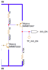
Can you provide the TPS82130 EN input circuit schematic?  I am looking at a TPS82130 circuit that generates 3.3V where VIN = 3.6V and the EN input is provided by the circuit below.  I am trying to work out why its EN signal 3V3_EN is sitting at approx. 2.3V and whether the TPS82130 device has been damaged because the EN input voltage may have exceeded it absolute maximum rating of VIN + 0.3V and it then being pulled down to 2.3V.

  • Hi Kevin,

    EN pin has an internal pulldown resistor of typically 400 kΩ when the device is disabled. I advise you run a simulation for this circuit to find the cause.

    Thank you.

    BR,

    Shipeng

  • I ran an LTspice simulation as you suggested using TPS82130_TRANS.LIB.

    The simulation showed the enable EN input being pulled up to 5V when the PNP transistor is turned on and not sitting at approx. 2.3V as per the actual circuit.  So either the TPS82130 model does not reflect reality and the simulation is not accurate or this is what the circuit should do and we do not have a problem as the EN input of 2.3V is within its operational limits.  Alternatively we gave damaged the TPS82130 converter.  Can you say which is the case?

  • Sorry for the typo, should have said "Alternatively we have damaged the TPS82130 converter.  Can you say which is the case?"

  • Hi Kevin,

    What your purpose to design the circuit outside EN pin? Do you want to control EN by a 5V signal? If yes, you can just use two resistors to divide the 5V voltage.

    In your circuit, when Q2 turns on, the 5V will go directly to EN pin. As VIN is only 3.6V, the internal ESD diode between VIN and EN will turns on, then 5V and 3.6V power rail are short. So the device can be damaged.

    I think you should add a resistor above Q2 to limit 5V go to EN pin directly.

    Hope this can help you.

    Best Regards,

    Shipeng

  • Thank you for your response.

    I didn't design the circuit so I cannot say why it was designed that way, maybe an oversight.  We have a number of these converters to provide 0V95, 1V0, 1V2, 1V8 & 3V3 for an FPGA. The circuit to the left of Q2 is a sequencer circuit, similar circuits are used for the other converters to power up the FPGA supplies in the correct sequence.  For some reason the 3V3 converter is powered from 3.6V whereas the 0V95, 1V0, 1V2 & 1V8 converters are powered from 5V so we don't have a problem with those but for some reason the 3V3 converter is powered from 3.6V.

    If by pulling EN to 5V we are turning on the ESD protection diodes between VIN and EN why is EN sitting at approx. 2.3V i.e. below VIN = 3.6V and not between VIN = 3.6V and 5V?

  • Hi Kevin,

    I think you can try to remove the IC and test the EN signal to confirm if the high-level is 5V. It's difficult to say what will happen when EN is higher than VIN. So we should try to modify the EN circuit to avoid make device in a wrong state.

    Thanks.

  • As per your email dated 19th March, unfortunately the matter is not resolved.  With our existing EN drive circuit we are seeing some units with the EN input sitting at approx. 2.3V and some units with it sitting at 4.5V implying the EN input ESD diodes are being turned on but have not failed.  We have a unit with it sitting at 4.49V that was used for our multiple power on/power off accelerated life test campaign.  Has there been a die change or do you uses different fabrication plants that might explain why some TPS82130 converters appear to be more robust than other?  Again we would appreciate the EN input circuit schematic so we can determine the reliability implications for our current design.

  • Hi Kevin,

    Because your application does violate our Absolute Maximum Ratings in datasheet, we won't guarantee our device can still operate normally under this situation. Some device now works just rely on our design margin. My advice is to modify your EN circuit.

    Thanks.

    Best Regards,

    Shipeng