This thread has been locked.

If you have a related question, please click the "Ask a related question" button in the top right corner. The newly created question will be automatically linked to this question.

LMQ66430: 3.3v Regulator short circuit issue

Part Number: LMQ66430

I am utilizing the LMQ66430 IC to regulate 9-24V down to 3.3V for an automotive application. My schematic for the IC is attached as is the schematic provided by WEBENCH. The issue I am seeing is the IC gets destroyed upon application of voltage (slowly ramping from 0V up to 12V). I am of the understanding that this IC has over temperature protection, however I have failed two ICS already due to temperature. Is there any possibility that something isn't spec'd properly or connected properly or should I assume that the GND pad is insufficient for providing enough thermal relief fast enough to prevent the IC from failing?

 0552.WBDesign3.pdfLMQ66430 Supply Schematic.pdf

  • Hi Adam,

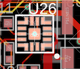
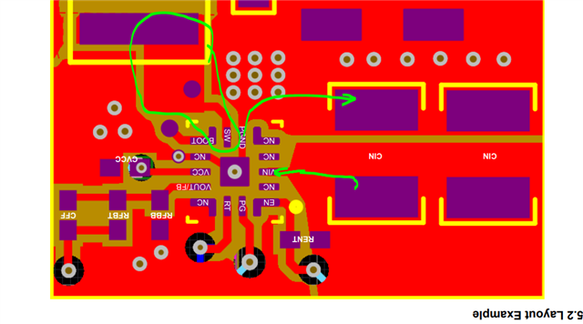
    Thank you for posting.  The schematic looks fine, but the layout needs improvement, although I haven't figured out how exactly the IC is damaged. Sorry the layout is not very clear to review, but I do found it is quite different from the commended layout in the datasheet.  I changed the orientation to be similar to your picture for easy comparison, and you can see in the recommended layout that the input capacitor is closely placed by the IC and the switching current takes a very short path from and to Cin.  In addition, SW is direct and short to the inductor; and PGND pin has direct connection to the ground polygon.  In yours, SW trace is zigzagging, and the PGND pin take the via hole in the under-pad, forcing the switching current to take a longer path.  All these introduces parasitic inductances along the PCB traces which would affect the normal operation of the circuit. Could you modify your layout by following the recommended one?

    Thanks,

    Youhao

  • Youhao,
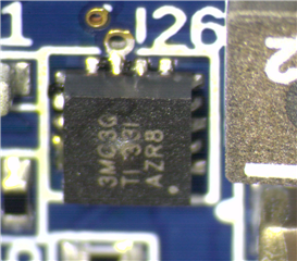
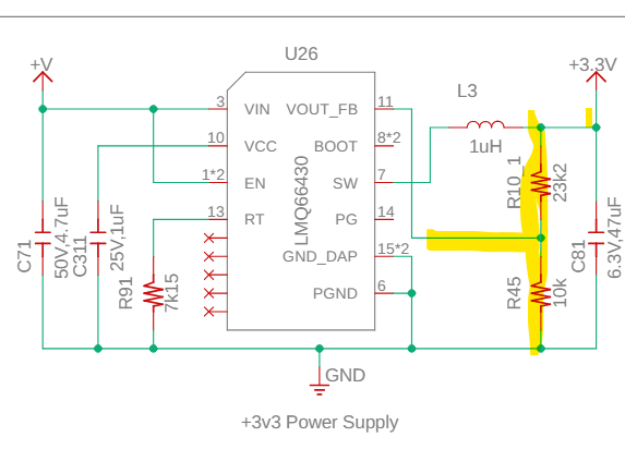
    I have recently also noticed that the IC in the circuit is the M variation not the R variation and thus instead if an RT pin it has a mode/sync pin. Could this be the potential issue leading to the damaged IC? See picture below and datasheet attached.
    As far as the layout issues you mentioned, would the parasitic inductance be capable of causing the failure mode I'm seeing? Another image of the layout is shown below.
  • Hi Adam,

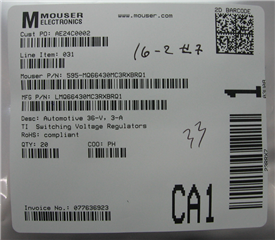
    Where did you get the M version of the part? According to the datasheet, LMQ66430 does not have a M version device. Can you share a photo picture of the label on the reel of tape?

    Thanks,

    Youhao

  • Youhao,

    The part is available from mouser: https://www.mouser.com/ProductDetail/Texas-Instruments/LMQ66430MC3RXBRQ1?qs=rQFj71Wb1eWZ6AyXDpSreA%3D%3D&gad_source=1&gclid=Cj0KCQiAhc-sBhCEARIsAOVwHuT1VbpITr8siGUTXfwiuQdyu7na0Dy4I4Zfhh9AFkbju0JeXyUB7SIaAnQaEALw_wcB

    We are currently reworking the PCBs to replace the IC from the link above with the IC in the below link:

    https://www.mouser.com/ProductDetail/Texas-Instruments/LMQ66430R5RXBR?qs=rQFj71Wb1eUBJjL24cjkfw%3D%3D

    Is there any possibility that this mix-up is the cause of the issues we are seeing?

    Adam

  • A reel was not purchased, here is the label from the distributor:

  • Hi Adam,

    Thank you. We are investigating it now.  Will update ASAP.

    Thanks,

    Youhao 

  • Hi Adam,

    Our expert of the device said these two devices could be swapped without causing damage.  However, since M version's MODE/SYNC pin is replaced with RT pin for the R version, and you are using RT function, I will suggest you to use the appropriate version.

    Or, you can verify this M version devices by either tying the MODE pin to VCC or GND and see if the issue is resolved.

    Thanks,

    Youhao

  • Youhao,

    The boards are currently being reworked to have the r chip populated.

    Is it possible that since we are applying low voltage to start the load draws no current since the voltage is too low and the inductor is drawing too much current and causing the IC to overheat?

    I just don't understand how the overtemperature protection doesn't prevent the IC from destroying itself. I can understand the parasitic inductance causing erratic output, but I don't know that it would destroy the IC.

    Adam

  • Hi Adam,

    Sorry I have not clue yet about how the IC is damaged.  It does not look like overheating under no load, unless there is a hidden error somewhere. 

    By the way, I forgot to explain the part number.  The R-version only exists for non-automotive version, and the M-version only for automotive version. My reply yesterday was referring to the non-automotive version datasheet.

     May I bother  you to capture a few waveform of the following circuit nodes:  VIN, SW, and Vout?  

    Thanks,

    Youhao

  • Youhao,

    I'll see what we can do when the reworked boards are back in our possession.

    Thanks for the support.

    Adam

  • Thank you Adam!!  Looking forward to the updates.

    Best Regards,

    Youhao

  • Youhao,

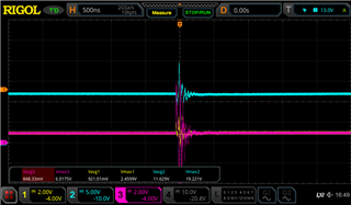
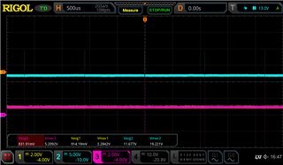
    Here are some scope traces:

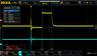
    The Blue is VIN (12V), the yellow is VOUT and the violet is SW, both are at about .9V. There appears to be a spike every ~1ms, close up also shown below. Any insights?

    Thanks in advance.

  • Youhao,

    Just wanted to check in and see of you had a chance to review the scope traces I uploaded last week.

    Adam

  • Hi Adam,

    Sorry for the delay due to the holidays.  We were off on Friday. 

    The spike indicates that the circuit is doing something, like a switching event.  Did you try short the MODE pin to GND or to VCC and see if the issue can be resolved?  I am afraid the RT resistor with an M version would lead to misbehavior.  Could you simply replace the RT with 0Ohm resistor?

    Thanks,

    Youhao

  • Youhao,

    The scope traces are for the R variation, we had the M variation removed as the PCB did not easily accommodate reworking the resistor. This trace was done with the load removed from the circuit to try and avoid any potential damage to the rest of the circuit. Could this be the cause? Do you foresee any damage being done if the load is applied?

    Adam

  • Hi Adam,

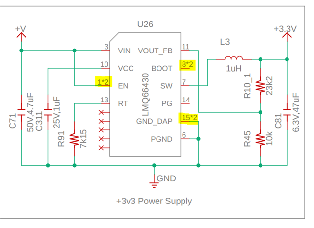
    Thank you for the explanation.  May I ask what do 1*2 and 8*2 mean in your schematic?   If "*2" just means an adjacent NC pin is also connected to these pins, then the circuit should work.  With or without load should not make much difference for being able to establish output regulation at ~3.3V other than getting stuck at 0.9V. I cannot see how the IC can be damaged unless I misunderstood "*2" in your drawing. 

    Thanks,

    Youhao

  • Youhao,

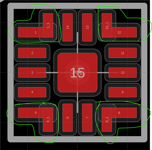
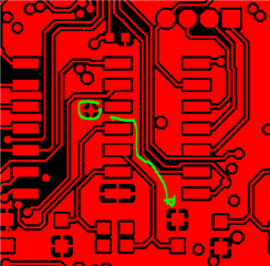
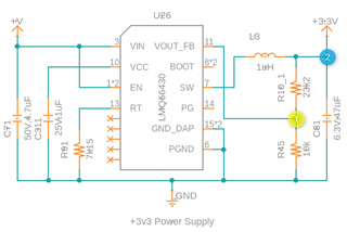
    The 2 just means that there are 2 pads in the footprint associated with this pin. This is done to overcome a shortfall of the design software which doesn't allow 'L' shaped pads to be created, see image below for clarification:

    Is there a reason you can think of that would cause us to be stuck at 0.9v? Is this the IC shutting down? Do you feel it is safe to connect the rest of the circuit, and perhaps take some more traces of that?

    Adam

  • Hi Adam,

    Thank you for the clarification.  This is a simple circuit and it should work.  I worry something wrong on the board but I cannot figure this out yet. I cannot trace the signal in your layout pictures.  How many vias do you have on the IC exposed pad? Could you share your layout files, layer by layer?

    Thanks,

    Youhao 

  • Youhao,

    I have attached the Gerber files for you to review.

    Adam6201.Gerber Files.zip

  • Hi Adam,

    Just let you know that I have received the file. Thank you for sharing.  Please allow me some time to review it, and I will get back to you ASAP.

    Thanks,

    Youhao

  • Hi Adam,

    Sorry for the delay.  It took me awhile to trace the signal. 

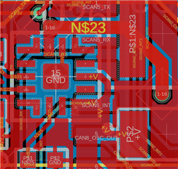
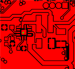
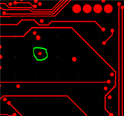
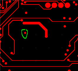
    I traced the IC under pad as well as the GND pin, and there is just a single via to the bottom side, then take a tiny trace to the input capacitor return node (see blow snapshots of layer by layer of the GND connection. Therefore, there is not much heatsink to cool the IC, when you slowing rise VIN, since the current at lower Vin would be higher, you would generate more losses during slow VIN ramp than faster ramp.  Yes the IC should have internal thermal shutdown to protect against self heating, but the IC can be easily damaged if the voltage exceeds the max rating. Since the current loop from Cin to the IC takes the tiny return trace zigzagging back to Cin, the PCB inductances could induce spike voltage when the IC is switching, and that can easily damage the IC. 

    In contrast, our EVM layout has short and direct connection between the IC underpad and GND pin to the PGND plane and also the Cin return terminal, the PCB heatsinking is much better to avoid overheating of the IC, and the PCB inductance is much smaller, therefore the induced spike voltage during switching would not damage the IC. 

    I don't see anything obviously wrong in your schematic.  I would suggest to modify the PCB by referring to our EVM layout example, and get better GND connection and PCB heatsinking.

    Hope this clarifies.

    Best Regard,

    Youhao

  • Youhao,

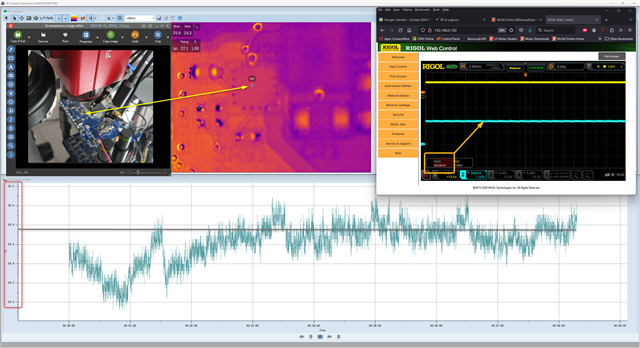
    We scoped the Cin pin to see if we are exceeding the max voltage of the device and we only reached 26V. We also utilized a thermal camera to see if we are overheating the device and as you can see, the output stays steady at .9V at does not get warm. Is there any other explanation for the output being stuck at .9V?

  • Hi Adam,

    Do you see a different phenomenon?  I remember you mentioned over temperature in your earlier posts, or this latest post is about a different failure mode?

    Is the first scope picture the zoomed in view of one of the switching edges?

    By the way, when you get 0.9Vout, can you measure FB to GND?  I mean on the IC side.

    Best Regards,

    Youhao

  • Youhao,

    We believe we had overtemperature with the M variant but we have not had such issue with the R variant, but now we are stuck at .9V on the output. All scope traces have been with the R variant.

    Adam

  • Hi Adam,

    I have the same frustration as you do, because I could not see any obvious mistake in your schematic nor layout that could explain the issue.  I just feel error is hidden because the circuit should support your application.  Let me consult our team and get back to you.

    Thanks,

    Youhao

  • Hi Adam,

    I discussed with colleagues and they suggest to test your IC on our EVM to see if it works correctly on the EVM, to make sure the IC was not compromised somehow.  Sorry to ask about this but could we exclude this possibility in debugging? 

    Thanks,

    Youhao

  • Youhao,

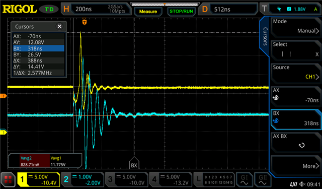
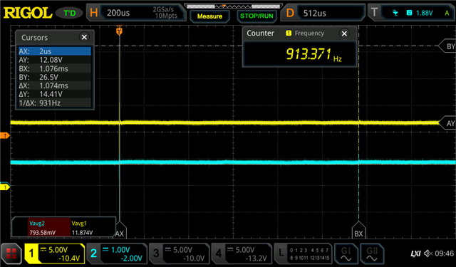
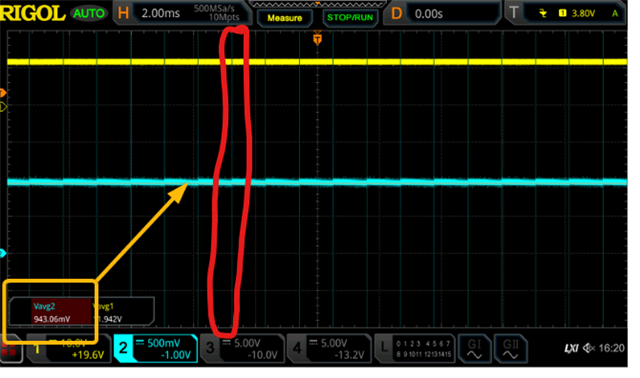
    Here is a scope trace of the FB pin, we have tried multiple boards and experience the same issue on all of them.

    Adam

  • Hi Adam,

    Thank you for the info.  May I assume CH1 is  FB voltage, and CH2 Vout?  According to  your schematic, FB produced by a resistor divider hence VFB is a fixed proportion of Vout.  How could it jumps up?  Could you trace the signal on your board and see if there is a hidden PCB error? 

    Thanks,

    Youhao

  • Youhao,

    We also tried the board with no resistors (fixed output of 5v) and we get the same result.

    Adam

  • Hi Adam,

    Sorry to hear but by same do you mean FB also jumps up like shown in above scope picture?  I am referring to the yellow trace. Is it FB? 

    Thanks,

    Youhao

  • I am wondering if the yellow trace in your scope picture is FB.  Could you confirm?

  • The yellow trace is FB yes, and blue is the output of the inductor as follows:


  • Hi Adam,

    It doesn't make sense if Vout is 0.9V flat but FB jumps up for some time.  I worry either there is a PCB error or the IC is somehow damaged. I will trace the FB signal on your layout file again.  Please allow me some time because I just got a new laptop and I am still trying to sort out things to set it properly.  

    Thanks,

    Youhao

  • Hi Adam,

    Very sorry that I still find the clue on the layout file that could explain the issue.   Could you ship a board to us so we can debug in our lab?   FYI: I will be ooo for next week and I will ask our colleague to monitor e2e and help arrange the shipping to us. 

    Also please accept my request of PMS. 

    Thanks,

    Youhao

  • Let me reach out to my customer and see if that can be arranged. I will report back early next week on this thread.

    Ada.

  • Thank you Adam!  Lets continue the talk until after I return to work.