Other Parts Discussed in Thread: HD3SS3212-Q1, HD3SS3212, TPS25830-Q1
 Hi E2E team,
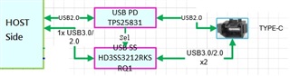
I would like to use TPS25831-Q1 and HD3SS3212-Q1 to implement an automotive product. A simplified block diagram is shown below:
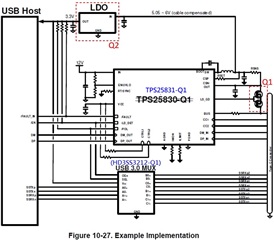
And Its planning is equivalent to Figure 10-27 in the TPS25831-Q1 datasheet.
Initially, I have two questions that I would like to consult:
Q1: There are two modes for current limit. (1)External MOSFET (2)Buck average current limit
Which one to choose based on what? I didn't find any clear instructions in the datasheet. Maybe I missed something, please remind me.
Q2: In Figure 10-27, a 3.3V LDO as a input power for USB3.0 Mux, and it's input come from TPS25831-Q1.
Are there any power sequence requirements for this? Since our system already has a buck output 3.3V inside, I would like to use it directly instead of adding another LDO to achieve it.
Is there anything I need to pay attention?