This thread has been locked.

If you have a related question, please click the "Ask a related question" button in the top right corner. The newly created question will be automatically linked to this question.

CSD19531Q5A: How to provide thermal heat dissipation for the mosfet

Part Number: CSD19531Q5A
Other Parts Discussed in Thread: CSD19532Q5B, TIDA-010042, CSD19535KTT, CSD18540Q5B, CSD19532KTT

Hi,

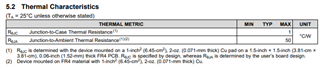
I need to reduce the heat generated on the mosfet. My converter is designed for a maximum current of 20A.What are the techniques for reducing the heat generated on the CSD19531Q5A. Whether attaching heatsink on the topside of the FET will transfer the heat. Please suggest me some techniques for reducing the heat on SMD mosfet.

Regards 

Cyril

  • Hello Cyril,

    Thanks for your interest in TI FETs. The main path to remove heat from the CSD19531Q5A is thru the thermal (drain) pad on the bottom of the package and into the PCB. You should maximize the PCB copper connected to the drain of the FET and if possible, use thermal vias in the drain pad to spread heat to the internal layers. The estimated thermal resistance, RθJA(top), is about 15°C/W. Heat sinking the top of the package might help to reduce the temperature if there is airflow across the heat sink fins.

    Reducing the power dissipation in the FET will also help to reduce the temperature. To reduce conduction loss, you can try a FET with lower on resistance FET, such as the CSD19532Q5B but it has higher charge/capacitance which may increase the switching losses. You can also parallel FETs to reduce conduction loss and spread the heat over a larger area. I'm assuming this goes into a switch-mode power supply and therefore lowering the switching frequency will reduce the switching loss. TI has a number of Excel-based FET selection tools for various applications that can be found in the "Tools" section of the app note at the link below. If you can share the application details, I can provide additional assistance to resolve your problem.

    https://www.ti.com/lit/an/slvafg3c/slvafg3c.pdf

    Best Regards,

    John Wallace

    TI FET Applications

  • Hi John,

    Thanks for your reply.

    I am using the reference design of TIDA-010042(old) for my application. In your reply, you have mentioned RθJA(top) is about 15°C/W. But when I checked data sheet, I have found it is 50°C/W. Whether it is a typing error.

    Regards,

    Cyril

  • Hi Cyril,

    Thanks for the updated information. TI specifies Max RθJA (junction to ambient) = 50°C/W and max RθJC (junction to bottom of case) = 1°C/W to the drain pad when mounted on 1 inch2 (6.45 cm2) of 2-oz. (0.071-mm thick) Cu. PCB in the FET datasheet. RθJC to the top of the package is an estimated value and is not specified in the datasheet. Please see link below for more information on how TI tests and specs thermal impedance for our FET packages.

    https://www.ti.com/document-viewer/lit/html/SSZTB80

    The reference design shows an output current of 16A and uses a 60V FET, CSD18540Q5B. You have selected a 100V FET and your output current is 20A. In general, the 5x6mm package can dissipate a maximum 3W depending on the board layout and ambient conditions. The estimated conduction loss for the CSD19531Q5A assuming TJ = 100°C is about 4.1W which greatly exceeds the package capability. Similarly, the CSD19532Q5B conduction loss is about 3.2W under the same conditions and exceeds the package capability. I think you are going to need to parallel FETs or use a FET in D2PAK such as CSD19532KTT (same FET die in a larger package) or CSD19535KTT (lower on resistance). Do you need to use 100V FET? A 60V FET is going to be lower resistance for the same die size.

    Thanks,

    John

  • Hi Cyril,

    Since I have not heard back from you, I assume your issue has been resolved and will close this thread.

    Thanks,

    John

  • Hi John,

    Sorry for the delay in response. I have been using TIDA-010042 old design based on CSD19531Q5A that was originally designed for 20A current. (TIDA-010042 GaN based mppt charger is designed for 16A).In old design switching fet was CSD19531Q5A and not CSD18540Q5B.Currently, TI have removed TIDA010042 old design files from site.

  • Hi Cyril,

    Thanks for the update. The current reference design documentation is available on TI.com at the link below. I was not involved in this design and do not know the history or why the FET was changed. Based on the schematic, it may be have been changed because the gate drive voltage for two of the FETs is only 5V and the CSD19531Q5A requires VGS >= 6V. The CSD18540Q5B requires VGS >=4.5V and is compatible with 5V gate drive. It is also much lower on resistance (2.2mΩ max vs. 6.4mΩ max at VGS = 10V) than the CSD19531Q5A and will support higher current. I am going to reassign this thread to the systems engineering team responsible for this reference design.

    https://www.ti.com/tool/TIDA-010042

    Thanks,

    John

  • Hi Cyril,

    I have the old design files for TIDA-010042, what do you want to know? The original fsw is 180kHz each, you may reduce the fsw to reduce the heat dissipation.

    Thanks,

    Bowen

  • Hello Bowen,

    Can I reduce the switching frequency, without the need to change the inductor value(22uH).

    Thanks,

    Cyril

  • Hi Cyril,

    Sorry for the late reply.

    Yes, you could try a lower frequency, for example 120kHz or 100kHz for this application.

    If you have any other questions, please feel free to ask.

    Best,

    Bowen