This thread has been locked.

If you have a related question, please click the "Ask a related question" button in the top right corner. The newly created question will be automatically linked to this question.

LM51231-Q1: Entered Bypass mode by mistake

Part Number: LM51231-Q1

Hi team,

I have a question about LM51231, please help me, thank you!
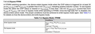
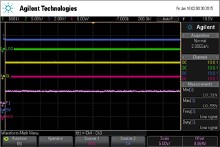
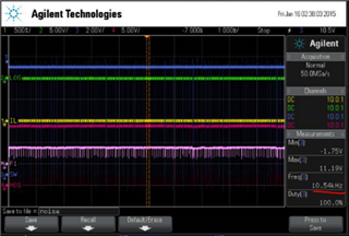
The input setting is 10.4v, the output is 10v, and it is configured in FPWM mode. The actual tested load current of CH1 IL in the picture is 500mA, and the sense resistor is 3mohm. KFB 20, VTRK 0.5v, according to the manual, it does not meet the enter bypass conditions, but it works in bypass mode. Why is this? Is it normal?

  • Hello Alan,

    Thanks for reaching out to us via e2e.

    I assume that the condition that you are showing is right after power-on.
    So, this shows what happens, when the controller has never started a switching cycle.
    Can you confirm that the LO pin has never become active / gone high?

    When at power-up Vin is higher than the commanded output voltage, the converter will never need to boost.
    In this case the LM51231 will start-up in bypass mode.

    The criteria that is mentioned in the table that you have added will need to be met when the controller shall transition from boost operation (both FETs toggling) to bypass mode.

    In a application which shall keep the output voltage above a certain level and where the input voltage is usually higher than this minimum level, it is expected that the controller will start-up in bypass mode.
    Otherwise, when the battery / input voltage gets disconnected and connected again, all load current would always flow across the body diode of the HS FET until it once needs to boost.

    Best regards
    Harry

    All information in this correspondence and in any related correspondence is provided “AS IS” and “with all faults” and is subject to TI’s Important Notice (www.ti.com/.../important-notice.shtml).

  • Hi Harry,

    I communicated with the customer today, and the situation tested by the customer did not occur during the start-up process. Instead, first set the input voltage below 10v, and the chip works in BOOST mode, and then gradually adjust the input voltage to a higher level. The customer's board will have anti-reverse and filter circuits. When the input is raised to about 10.4v, a lower tube will appear. off, the top tube is 100% on. If the input voltage is adjusted higher, at 11.1v, the upper tube will turn off. Please help to confirm, why does it enter bypass mode at this time?

  • Hi Alan,

    as many people are already out of the Easter vacation, I would like to wait for Harry to comment here next week.

    Best regards,

     Stefan

  • Hi Stefan,

    Sure,At the end of the holiday, please take a look at the following question:

    There is another question about noise. I switched to FPWM mode. When the input just exceeds 10v and the load is about 360mA, the board will have a slight noise. Below is a measured waveform for reference. Is there any way to avoid this low frequency from the source? Thanks!

  • Hi Stefan,

    Is Harry's vacation over? Can you help update the analysis of related issues?

  • Hello Alan,

    Thanks for your patience.

    Can you please explain the reason why you are using the LM51231 rather than the LM5123?

    Regarding the noise:
    Are you sure that this noise is seen on any of the signals and not just an artefact of the math function?
    If you can see it on a measured signal, which one is it (HO or SW)?

    Thanks and regards
    Harry

  • Hi Harry,

    This is carry over project in our side, I need to further check with my colleague why not use LM5123. 

    In the picture, HOG is HO gate signal, LOG is LO gate signal, if enlarge the picture, you can see that each channel has switch action. i am sure that is not an artefact of the math function. In this case, we can also hear the noise when close to board nearly. Thanks a lot.

  • Hello Bruce,

    At light load and when the zero current detection is not met, the controller can keep the High side FET turned ON, which looks similar to the bypass mode.
    When you further increase the input voltage, the following will happen:
    - LM51231: The controller needs to see 10% of the peak current on the sense resistor to be able to switch to bypass mode. Therefore, with no load or a small load you will see that both FETs get turned OFF when you exceed 11.1V.
    - LM5123: The LM5123 does not have this requirement for a minimum positive current to go to bypass mode. But it has lower threshold voltages to go in and out of bypass. And the SYNC/DITHER/VH/CP pin needs to be set to High level (VCC) to enable the charge pump.

    When the input voltage is close to the output voltage, the converter still needs to boost a little bit to compensate for the voltage drop on the high side FET and for losses.
    The low frequency pulses that you see is the result of the pulse skipping that will happen in such a case.
    There is not really anything that you can do to avoid that. The frequency can maybe get shifted a bit by choosing different size output capacitors.

    Audible noise can be generated by the inductor, but also by the ceramic capacitors.
    As a test, you can remove the inductor from the board and connect it via thick flexible wires (but not too long wires).
    This way there is a mechanical disconnect for the vibrations and you can better distinguish the source of the noise.

    All information in this correspondence and in any related correspondence is provided “AS IS” and “with all faults” and is subject to TI’s Important Notice (www.ti.com/.../important-notice.shtml).

    Best regards
    Harry.