This thread has been locked.

If you have a related question, please click the "Ask a related question" button in the top right corner. The newly created question will be automatically linked to this question.

UCC28070A: Unusual Current-sense signal slope (and inductors that are too hot)

Part Number: UCC28070A

Hello,

The project we're working on is a Power Factor Corrector, PFC board for a customer that uses them to power ozone-reactors for industrial washing machines.

More specifically, it is an interleaved boost PFC where the logic is powered externally with 15V. It is modelled after this evaluation board from Infineon EVAL-PFC5KIKWWR5SYS. The PFC output is connected to a 4.3 kW load for testing purposes.

When performing tests, we noticed that the inductors reached quite high temperatures compared to that of the reference design from Infineon. Interestingly, one of the inductors showed a different temperature than the other: one (Inductor A) being at 105 and the other (Inductor B) at 70 degrees celcius.

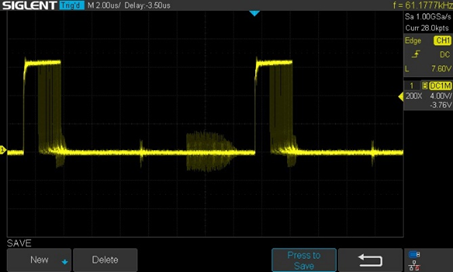
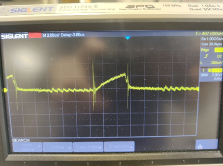
Measuring the gate signals GA and GB on an oscilloscope showed a difference in maximum duty cycle that the gate drivers outputted. The gate driver inputs (GDA and GDB) from the PFC IC (UCC28070A) have duty cycles that match their respective GA and GB gate driver outputs.

GDB (left) and GDA (right). Measured while having the PFC board connected to a 4,3kW load.


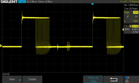
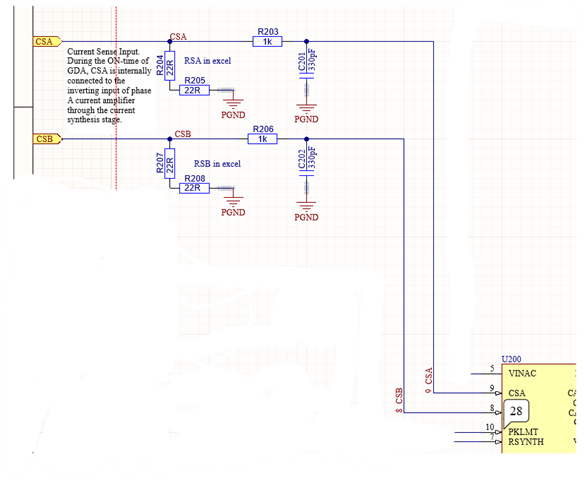
We assumed that it had to do with the feedback signals. The current-sense signals, CSA and CSB (coming out from the CS transformers) can be configured individually with passive components so we measured their waveforms. Here is the schematic with the CSA and CSB signals. we probed right above the two 22 ohm resistors.

Measuring CSA and CSB on the oscilloscope showed a difference in the voltage slope. Here are the waveforms, CSA (left) and CSB (right)


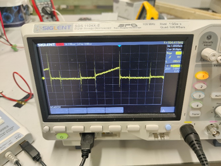
Why is the second CSB voltage sloped like that? It also seems to drop before reaching the IGBT switching spike which also seems wrong. Is this related to the problem with the Inductor heating up differently? We have replaced the passive components but the problem persists.

I appreciate any help I can get and hope I have made myself clear. I am quite new to electronics, not to mention power electronics so forgive me any unclarities.

  • Hello Jonathan, 

    Thank you for your question on current-sensing for the UCC28070A PFC controller. 

    From the GDA and GDB waveforms, one can see that GDA minimum on-time (for the test conditions) is roughly 3x as long as for GDB.
    It makes sense, then, that inductor A is much hotter, because the increased on-time allows a much higher current level in phase-A than in Phase-B. 
    Ideally, GDA and GDB (and the respective inductor currents) should be identical.   
    Aside from explaining the difference between inductor temperatures, I can't guess why your customer's inductors run hotter than those in the Infineon Eval board (assuming same test conditions), except to speculate that maybe the Infineon inductors are better designed for lower losses than your customer's design.   

    Now, the question is why GDA on-time is so much wider than that of GDB.  Both PWM comparators receive the same IMO signal and both channel synthesizers use the same RSYNTH-programmed downslope, so the difference must come from the CSA vs. CSB signals.  
    As you note, the Vcsb signal has a distorted slope and shape compared to Vcsa.  

    It is not clear that the Vcsb signal is captured at the same instantaneous point in the line cycle as Vcsa.  Capturing 2 channels simultaneously would resolve that question, but given the CSB distortion shown, I suspect that overall Vcsb is attenuated.  Since the current amps and PWM comparators adjust PWM to match Vimo, I believe that PWM-B is larger than PWM-A because Vcsb is smaller than Vcsa for the same Vimo reference.   

    Now, the question becomes what is causing the Vcsb signal to be distorted.  (This assumes that Vcsa is correct, and it certainly looks more correct than Vcsb.)
    First, please remove capacitor C12 (330pF) from the cathode of the T1 transformer output diode.  Do the same for the other phase (not shown). 
    There should be no capacitance there. 
    Second, verify that the Vcsa and Vcsb cycle-by-cycle signals are an accurate scaling of the actual inductor currents in each cycle.  Compare them at several point along the rectified AC line (at zero-crossings, a little up the sine wave, more up the sine wave, more up, near the peak, at the peak, and mirror the points down the sine.)    
    The purpose is to detect whether the CSx signal may be reduced by excessive magnetizing current (Imag) in the current-sense transformer.  This current can "steal" signal level from the sense resistors (RSA, RSB) and make the inductor current look lower than it really is.  
    Excess Imag comes from insufficient volt-second reset during the gate-drive off times.  
    Please read Section 7.2.2.7 of the UCC28070A datasheet for more information on this topic. 

    Note that too much Imag may not be the only root cause of the CSx signal difference.  Other causes may be due to incorrect component values installed onto the prototype board. 
    The schematic values may be correct but one of the actual board values may be wrong. Or a broken connection (open circuit or short circuit) may exist, etc. 
    Check each part in the current sense path to verify that it is correct, and the signal is correct.
    Also, verify that both inductors are identical.  Swapping La and Lb can prove that the problem exists at or after the CT, not following the inductor itself. 

    Debug by assuming that all the PFC signals and operation in the two phases should be identical (except phase-shifted), and pursue investigation where they are not. 

    Regards,
    Ulrich