This thread has been locked.

If you have a related question, please click the "Ask a related question" button in the top right corner. The newly created question will be automatically linked to this question.

TPS25762-Q1: TPS25762-Q1: Question regarding BC1.2 and D+, D-, FW update through USB endpoint

Part Number: TPS25762-Q1
Other Parts Discussed in Thread: TPS254900A-Q1

Hello Team!

Can you kindly advise:

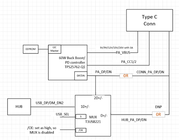
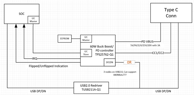
1. We would like to connect PA_DP/PA_DM to USB port D+/D- for BC1.2. HOST IC also need to connect with USB connector D+/D- for USB2.0 normal communication. Do you have any recommendation for the D+/D- connection for USB signal integrity? I draw a block diagram as followed. Please give advice for the USB 2.0 connection.

Many thanks,

Jeffery

  • Hi Jeffrey,

    Have you seen how we've implemented what you are describing on the TPS25762Q1EVM? The EVM's schematic is included in the EVM User's Guide.

    Please take a look and let me know if you have any questions on the design.

    BR,

    Seong

  • Hi Seong,

    I have checked  TPS25762Q1EVM and its user's guide. I did not find the solution for the question. Can you give a block diagram for your solution to my following questions?

    1. Make the TPS25762 support BC1.2 and PD3.

    2. Also support HOST SOC communicate with the remote usb device.

    3. Make the firmware update through USB-C port.

    Many thanks,

    Jeffery

  • I draw a diagram according to  TPS25762Q1EVM and its schematics as followed, please help confirm how to solve the above three question?

    Many thanks,

    Jeffery

  • Hi Jeffrey,

    Your block diagram answers the three questions. You've added the MUX to be able to route the DP/DM lines to either the TPS25762-Q1 or the SoC. Just note that TVSP1 must be used to boot the device in USB Endpoint FW Update mode. See Section 9.3.2 in the datasheet.

    For USB2.0 high speed signal conditioning inquiries, please leverage the Interface Forums here.

    Let us know if you have any other questions.

    Thanks and best regards,

    Seong 

  • Hi Seong,

    My concern is on this points: If we route the DP/DM lines to TPS25762, BC1.2 DCP mode is realized, but the DP/DM is not connected to SOC. We can not make BC1.2 and USB communication happen at the same time just as "Charging Downstream Port (CDP)".  Is my understanding correct?

    Please give some suggestion for this point.

    My thanks,

    Jeffery

  • Hi Seong,

    I have another question is for the I2C logic(VDD) when the TVSP is set as index 7(Rtvsp:8.45kohm)? As you know the EEPROM is on the I2C1 of TPS25762, it is powered by LDO_3V3 of TPS25762. So the I2C logic for I2C1 is always 3.3V. The I2C logic(VDD) configured by index 7 is 1.8V, it is for I2C2 of TPS25762?

    Is my understanding correct?

    My thanks,

    Jeffery

  • Hi Seong,

    If TVSP is set as index 2, so TPS25762 boot from external EEPROM on the I2C1 interface, the pull up voltage of I2C1 is 3V3. While the I2C2 is connected to MCU, and the pulled up voltage of I2C2 is 1.8V, is it ok?

    For the firmware update, please help answer the following questions:

    And on the above configuration, can MCU make the firmware update for EEPROM through I2C2?

    Before MCU run the firmware update through I2C2, do MCU need to change TVSP to index 8 "Firmware Update"?

    Many thanks,

    Jeffery

  • Hi Jeffery,

    Due to the holiday, many device experts are currently out of the office. When they return they will look into this and provide a response. Please expect some delay accordingly.

    Thanks,
    Field

  • Jeffrey,

    1. Correct, use the TPS25762-Q1 for only PD in this case. If BC1.2 is needed, a BC1.2 controller should be added, such as the TPS254900A-Q1 so that DP/DM are routed only to the TPS254900A-Q1 and host IC. This is unless the host IC is integrated with a BC1.2 controller.
    2. The VDD voltage level applies to both I2C1 and I2C2 input voltage thresholds. With TVSP7 selected and using a 3.3V EEPROM, there should not be any issues if the I2C1 lines are pulled up to 3V3 with the correct resistor values. Section 7.16 in the datasheet shows the small voltage difference of when the clock is pulled low when VDD is 1.8V or 3.3V, so do keep this spec in mind.
    3. Same thing with the I2C2 line pulled up to 1.8V. With the correct resistor values, there should not be any problems as long as the MCU supports 1.8V logic.  
    4. No, the EEPROM can only be connected to I2C1. To boot the device in Firmware Update mode, TVSP8 must be selected before a POR or soft-reset. Note that the device will stay in this mode even after successfully programming the EEPROM. The TVSP must then be changed to either Index 0, 2, 4, or 6 before another POR or soft-reset to boot the device in EEPROM mode for normal operation with the new patch bundle.

    BR,

    Seong

  • Hi Seong,

    Thanks a lot!

    I appreciate your great help!

    Jeffery

  • For the I2C logic level, I still have a question. The spec.7.16 for Vil and Vih are confused. There are two values for these two items.  One line is" Min Vih is 1.3V." Does it stand for value of  ”VDD = 1.8V” ?or it applied to two case “VDD=3.3V or VDD =1.8V”?

  • Hi Seong,

    I have another understanding for the I2C logic level, If we select the TVSP as index 2, and TPS25762 boot from EEPROM, and it also defines the I2C logic level is 1.8V for both I2C1 and I2C2. But we can pull up I2C1 to 3.3V, and pull up I2C2 to 1.8V. Because the input level logic thresholds is for 1.8V logic. TPS25762's I2C can work correctly. Is my understanding correct?

    And on this configuration: MCU connect TPS25762 through I2C2 with 1.8V pull up and TPS25762 connect to EEPROM through I2C1 with 3.3V pull up.

    if we want to use MCU to update firmware of TPS25762's EEPROM, we need to change the TVSP to index 8 first. But according to the Rtvsp table, index 8 also defines the I2C logic level is 3.3V.  That will conflicts with previous "Pull up I2C2 to 1.8V", how to solve this issue?

    Thanks,

    Jeffery 

  • Hi Jeffrey,

    For the I2C logic level, I still have a question. The spec.7.16 for Vil and Vih are confused. There are two values for these two items.  One line is" Min Vih is 1.3V." Does it stand for value of  ”VDD = 1.8V” ?or it applied to two case “VDD=3.3V or VDD =1.8V”?

    • Yes, the 0.54V input low and 1.3V input high specification is when VDD=1.8V. Apologies - we'll need to update the datasheet to make this clearer.

    I have another understanding for the I2C logic level, If we select the TVSP as index 2, and TPS25762 boot from EEPROM, and it also defines the I2C logic level is 1.8V for both I2C1 and I2C2. But we can pull up I2C1 to 3.3V, and pull up I2C2 to 1.8V. Because the input level logic thresholds is for 1.8V logic. TPS25762's I2C can work correctly. Is my understanding correct?

    • Yes, that is correct. As long as the appropriate resistor values are used so the lines can be reliably pulled low under 0.54V, there won't be any problems. 

    And on this configuration: MCU connect TPS25762 through I2C2 with 1.8V pull up and TPS25762 connect to EEPROM through I2C1 with 3.3V pull up.

    if we want to use MCU to update firmware of TPS25762's EEPROM, we need to change the TVSP to index 8 first. But according to the Rtvsp table, index 8 also defines the I2C logic level is 3.3V.  That will conflicts with previous "Pull up I2C2 to 1.8V", how to solve this issue?

    • In this case, I2C level shifters are recommended.

    BR,

    Seong

  • Many thanks!