


Hi,
I've got two questions regarding TPS2640 eFUSE. I noticed some discrepancies between the documentation for the IC and the evaluation board, hence the questions.
1. In the diagram of the evaluation board, a TVS diode (D8) is placed between the power IN and OUT pins. Is it necessary? Why was it added there?
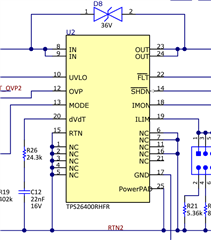
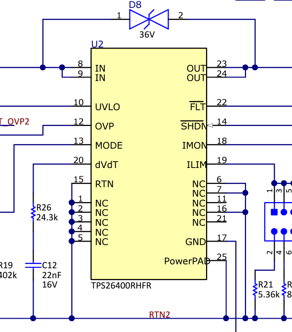
2. In the same photo you can see that on the evaluation board some NC pins are connected to the RTN potential. The integrated circuit documentation states not to connect them. What does this eval board scheme mean? Should these pins be connected, and if so, which ones exactly?
Thank you in advance for all answers!
Slawomir Z
